ZHCSEV1A February   2016  – March 2016 TPS62770

PRODUCTION DATA.  

  1. 特性
  2. 应用
  3. 说明
  4. 修订历史记录
  5. Pin Configuration and Functions
    1. 5.1 Output Voltage Setting Step-Down Converter
  6. Specifications
    1. 6.1 ESD Ratings
    2. 6.2 Thermal Information
    3. 6.3 Electrical Characteristics
    4. 6.4 Typical Characteristics
  7. Detailed Description
    1. 7.1 Overview
    2. 7.2 Functional Block Diagram
    3. 7.3 Feature Description
      1. 7.3.1 Step-Down Converter Device
        1. 7.3.1.1 DCS-Control™
        2. 7.3.1.2 Output Voltage Selection with pins VSEL1-VSEL3
        3. 7.3.1.3 CTRL / Output Load
        4. 7.3.1.4 Output Discharge At Pins VO1 And LOAD
        5. 7.3.1.5 Undervoltage Lockout UVLO
        6. 7.3.1.6 Short Circuit Protection
      2. 7.3.2 Step-Up Converter Device
        1. 7.3.2.1 Under-Voltage Lockout
        2. 7.3.2.2 Output Disconnect
        3. 7.3.2.3 12V Fixed Output Voltage
        4. 7.3.2.4 Mode Selection With Pin BM
        5. 7.3.2.5 Output Overvoltage Protection
        6. 7.3.2.6 Output Short Circuit Protection
        7. 7.3.2.7 PWM to Analog Converter AT PIN EN2/PWM
    4. 7.4 Device Functional Modes
      1. 7.4.1 Step-Down Converter
        1. 7.4.1.1 Enable and Shutdown
        2. 7.4.1.2 Power Save Mode Operation
        3. 7.4.1.3 PWM Mode Operation
        4. 7.4.1.4 Device Start-up and Soft Start
        5. 7.4.1.5 Automatic Transition Into 100% Mode
      2. 7.4.2 Step-Up Converter
        1. 7.4.2.1 Enable and Shutdown
        2. 7.4.2.2 Soft Start
        3. 7.4.2.3 Power Save Mode
        4. 7.4.2.4 PWM Mode
        5. 7.4.2.5 Constant-Current Step-Up Mode Operation
        6. 7.4.2.6 Constant-Voltage Step-Up Mode Operation
  8. Application and Implementation
    1. 8.1 Application Information
    2. 8.2 Typical Application
      1. 8.2.1 System and PMOLED Supply
        1. 8.2.1.1 Design Requirements
        2. 8.2.1.2 Application Curves Step-Down Converter
        3. 8.2.1.3 Application Curves Step-Up Converter Constant 12 V/15 V Output Voltage
      2. 8.2.2 Step-Up Converter with 5-V Output Voltage
        1. 8.2.2.1 Design Requirements
        2. 8.2.2.2 Application Curves
      3. 8.2.3 Step-Up Converter Operating with Constant Output Current
        1. 8.2.3.1 Design Requirements
        2. 8.2.3.2 Detailed Design Procedure
          1. 8.2.3.2.1 Setting The Output Voltage Of The Step-Down Converter
          2. 8.2.3.2.2 Programming the Output Voltage Of The Step-Up Converter
          3. 8.2.3.2.3 Recommended LC Output Filter
          4. 8.2.3.2.4 Inductor Selection Step-Down Converter
          5. 8.2.3.2.5 Inductor Selection Step-Up Converter
          6. 8.2.3.2.6 DC/DC Input and Output Capacitor Selection
        3. 8.2.3.3 Application Curves
  9. Power Supply Recommendations
  10. 10Layout
    1. 10.1 Layout Guidelines
    2. 10.2 Layout Example
  11. 11器件和文档支持
    1. 11.1 器件支持
      1. 11.1.1 开发支持
        1. 11.1.1.1 Third-Party Products Disclaimer
    2. 11.2 文档支持
      1. 11.2.1 相关文档 
    3. 11.3 商标
    4. 11.4 静电放电警告
    5. 11.5 Glossary
  12. 12机械、封装和可订购信息

封装选项

机械数据 (封装 | 引脚)
散热焊盘机械数据 (封装 | 引脚)
订购信息

10 Layout

10.1 Layout Guidelines

  • As for all switching power supplies, the layout is an important step in the design. Care must be taken in board layout to get the specified performance.
  • If the layout is not carefully done, the regulator could show poor line and/or load regulation, stability issues as well as EMI problems and interference with RF circuits.
  • It is critical to provide a low inductance, impedance ground path. Therefore, use wide and short traces for the main current paths.
  • The input capacitor should be placed as close as possible to the IC pins VIN and GND. The output capacitors should be placed close between VO1/2 and GND pins.
  • The VO1/2 line should be connected to the output capacitor and routed away from noisy components and traces (e.g. SW line) or other noise sources.
  • See Figure 44 and Figure 45 for the recommended PCB layout.

10.2 Layout Example
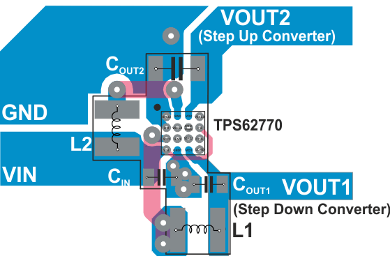
TPS62770 TPS62770_SolSize.gif Figure 44. Recommended PCB Layout with 12 V Fixed VOUT2
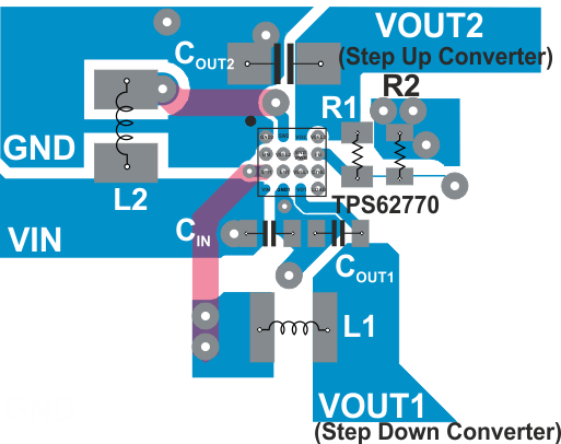
TPS62770 TPS62770_Flexible.gif Figure 45. Recommended PCB Layout with Adjustable VOUT2