ZHCSEV1A February 2016 – March 2016 TPS62770
PRODUCTION DATA.
- 1 特性
- 2 应用
- 3 说明
- 4 修订历史记录
- 5 Pin Configuration and Functions
- 6 Specifications
- 7 Detailed Description
-
8 Application and Implementation
- 8.1 Application Information
- 8.2
Typical Application
- 8.2.1 System and PMOLED Supply
- 8.2.2 Step-Up Converter with 5-V Output Voltage
- 8.2.3
Step-Up Converter Operating with Constant Output Current
- 8.2.3.1 Design Requirements
- 8.2.3.2
Detailed Design Procedure
- 8.2.3.2.1 Setting The Output Voltage Of The Step-Down Converter
- 8.2.3.2.2 Programming the Output Voltage Of The Step-Up Converter
- 8.2.3.2.3 Recommended LC Output Filter
- 8.2.3.2.4 Inductor Selection Step-Down Converter
- 8.2.3.2.5 Inductor Selection Step-Up Converter
- 8.2.3.2.6 DC/DC Input and Output Capacitor Selection
- 8.2.3.3 Application Curves
- 9 Power Supply Recommendations
- 10Layout
- 11器件和文档支持
- 12机械、封装和可订购信息
7 Detailed Description
7.1 Overview
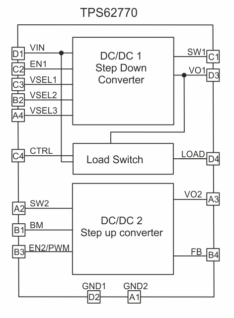
The TPS62770 is a tiny power solution for wearable applications including a 370nA ultra low Iq step-down converter, a slew rate controlled load switch and a dual mode step-up converter. The output voltage of the step-down converter can be selected with three VSEL pins between 1.0 V, 1.05 V, 1.1 V, 1.2 V, 1.8 V, 1.9 V, 2.0 V and 3.0 V.
The dual mode step-up converter can generate a constant output voltage up to 15 V, such as PMOLED supply or, a constant output current, such as LED back light supply.
7.2 Functional Block Diagram
7.3 Feature Description
7.3.1 Step-Down Converter Device
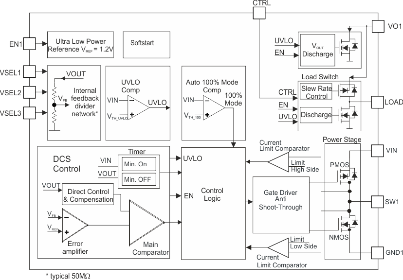 Figure 4. Block diagram Step-Down Converter with Load Switch
7.3.1.1 DCS-Control™
TI's DCS-Control™ (Direct Control with Seamless Transition into Power Save Mode) is an advanced regulation topology, which combines the advantages of hysteretic and voltage mode control. Characteristics of DCS-Control ™ are excellent AC load regulation and transient response, low output ripple voltage and a seamless transition between PFM and PWM mode operation. DCS-Control™ includes an AC loop which senses the output voltage (VO1 pin) and directly feeds the information to a fast comparator stage. This comparator sets the switching frequency, which is constant for steady state operating conditions, and provides immediate response to dynamic load changes. In order to achieve accurate DC load regulation, a voltage feedback loop is used. The internally compensated regulation network achieves fast and stable operation with small external components and low ESR capacitors. The DCS-Control™ topology supports PWM (Pulse Width Modulation) mode for medium and high load conditions and a Power Save Mode at light loads. Since DCS-Control™ supports both operation modes within one single building block, the transition from PWM to Power Save Mode is seamless with minimum output voltage ripple. The step-down converter offers both excellent DC voltage and superior load transient regulation, combined with low output voltage ripple, minimizing interference with RF circuits.
7.3.1.2 Output Voltage Selection with pins VSEL1-VSEL3
The step-down converter doesn't require an external resistor divider network to program the output voltage. The device integrates a high impedance feedback resistor divider network that is programmed by the pins VSEL1-3. It supports an output voltage range from 1.0 V to 3.0 V. The output voltage is programmed according to Output Voltage Setting Step-Down Converter . The output voltage can be changed during operation. This can be used for simple dynamic output voltage scaling.
7.3.1.3 CTRL / Output Load
With the CTRL pin set to high, the integrated loadswitch is activated and connects the LOAD pin to the VO1 pin to power up an additional sub-system. The load switch is slew rate controlled to support soft switching and not to impact the regulated output VO1. If CTRL pin is pulled to GND, the LOAD pin is disconnected from the VO1 pin and internally connected to GND by an internal discharge switch. The CTRL pin can be controlled by a micro controller.
7.3.1.4 Output Discharge At Pins VO1 And LOAD
Both the VO1 pin and the LOAD pin feature a discharge circuit to connect each rail to GND, once they are disabled. This feature prevents residual charge voltages on capacitors connected to these pins, which may impact proper power up of the main- and sub-system. With CTRL pin pulled to low, the discharge circuit at the LOAD pin becomes active. With the EN pin pulled to low, the discharge circuits at both pins VO1 and Load are active. The discharge circuits of both rails VO1 and LOAD are associated with the UVLO comparator as well. Both discharge circuits become active once the input voltage VIN has dropped below the UVLO comparator threshold VTH_UVLO- and the UVLO comparator triggers.
7.3.1.5 Undervoltage Lockout UVLO
The UVLO circuit shuts down the device if the input voltage VIN drops to typical 1.9V. The device will start up at an input voltage of typ. 2.1V.
7.3.1.6 Short Circuit Protection
The step-down converter integrates a current limit on the high side, as well on the low side MOSFETs to protect the device against overload or short circuit conditions. The peak current in the switches is monitored cycle by cycle. If the high side MOSFET current limit is reached, the high side MOSFET is turned off and the low side MOSFET is turned on until the switch current decreases below the low side MOSFET current limit. Once the low side MOSFET current limit trips, the low side MOSFET is turned off and the high side MOSFET turns on again.
7.3.2 Step-Up Converter Device
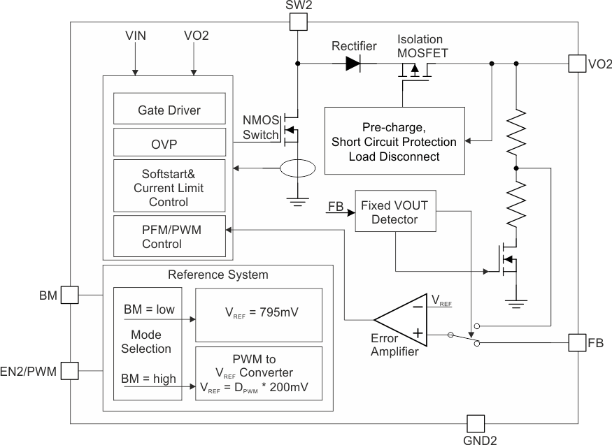 Figure 5. Block Diagram Step-Up Converter
The step-up converter is designed for applications requiring voltages up to 15V from an Li-Ion battery and tiny solution size such as PMOLED displays or LED back light for small size LCD displays. The step-up converter operates in two different modes, either as constant output voltage step-up converter operating with 0.8V internal reference or as a constant output current step-up converter operating with a reduced internal reference voltage of 200mV. The block integrates power switch, input/output isolation switch, and power diode.
7.3.2.1 Under-Voltage Lockout
See section Undervoltage Lockout UVLO
7.3.2.2 Output Disconnect
One common issue with conventional step-up regulators is the conduction path from input to output even when the device is disabled. It creates three problems, which are inrush current during start-up, output leakage current during shutdown and excessive over load current. The step-up converter has an integrated isolation (load disconnect) switch, which is turned off under shutdown mode and over load conditions, thereby opening the current path to the output VO2. Thus the device can truly disconnect the load from the input voltage and minimize the leakage current during shutdown mode.
7.3.2.3 12V Fixed Output Voltage
The step-up converter features an internal default 12-V output voltage setting by connecting the FB pin to the VIN pin. Therefore no external resistor divider network is required minimizing the total solution size.
7.3.2.4 Mode Selection With Pin BM
The step-up converter can operate in two different modes. With pin BM = low the device regulates to a constant output voltage, with BM = high, the device can regulate a constant output current. Further details in section Constant-Current Step-Up Mode Operation and section Constant-Voltage Step-Up Mode Operation. The operation mode need to be selected before the device is enabled. The pin BM may not be changed during operation.
7.3.2.5 Output Overvoltage Protection
When the output voltage exceeds the OVP threshold of 17.7 V, the device stops switching. Once the output voltage falls 0.8 V below the OVP threshold, the device resumes operation again.
7.3.2.6 Output Short Circuit Protection
The step-up converter starts to limit the output current whenever the output voltage drops below 4 V. When the VOUT pin is shorted to ground, the output current is limited. This function protects the device from being damaged when the output is shorted to ground.
7.3.2.7 PWM to Analog Converter AT PIN EN2/PWM
In constant current step-up mode operation two control functions are associated with the pin EN2/PWM:
a) Enable/ disable of the step-up converter
b) PWM to analog conversion to scale the internal reference voltage.
The internal reference voltage scales proportional with the duty cycle of the PWM signal applied at the pin EN2/PWM. More details in section Constant-Current Step-Up Mode Operation.
7.4 Device Functional Modes
7.4.1 Step-Down Converter
7.4.1.1 Enable and Shutdown
The step-down converter is turned on with EN1 = high. With EN1 = low the step-down converter is turned off. This pin must be terminated.
7.4.1.2 Power Save Mode Operation
At light loads, the device operates in Power Save Mode. The switching frequency varies linearly with the load current. In Power Save Mode the device operates in PFM (Pulse Frequency Modulation) that generates a single switching pulse to ramp up the inductor current and recharges the output capacitor, followed by a sleep period where most of the internal circuits are shutdown to achieve lowest operating quiescent current. During this time, the load current is supported by the output capacitor. The duration of the sleep period depends on the load current and the inductor peak current. During the sleep periods, the current consumption is reduced to 360 nA. This low quiescent current consumption is achieved by an ultra low power voltage reference, an integrated high impedance feedback divider network and an optimized Power Save Mode operation.
7.4.1.3 PWM Mode Operation
At moderate to heavy load currents, the device operates in PWM mode with continuos conduction. The switching frequency is up to 1.6 MHz with a controlled frequency variation depending on the input voltage and load current. If the load current decreases, the converter seamlessly enters Power Save Mode to maintain high efficiency down to very light loads.
7.4.1.4 Device Start-up and Soft Start
The step-down converter has an internal soft start to minimize inrush current and input voltage drop during start-up. Once the device is enabled the device starts switching after a typical delay time of 1 ms. Then the soft start time of typical 700 μs begins with a reduced current limit of typical 150mA. When this time expires the device enters full current limit operation.
7.4.1.5 Automatic Transition Into 100% Mode
Once the input voltage comes close to the output voltage, the DC/DC converter stops switching and enters 100% duty cycle operation. It connects the output VOUT via the inductor and the internal high side MOSFET switch to the input VIN, once the input voltage VIN falls below the 100% mode enter threshold, VTH_100-. The DC/DC regulator is turned off, switching stops and therefore no output voltage ripple is generated. Because the output is connected to the input, the output voltage follows the input voltage minus the voltage drop across the internal high side switch and the inductor. Once the input voltage increases and trips the 100% mode exit threshold, VTH_100+ , the DC/DC regulator turns on and starts switching again.
7.4.2 Step-Up Converter
7.4.2.1 Enable and Shutdown
The device is turned on with EN2/PWM = high. With EN2/PWM = low the device enters shutdown mode. In constant current step-up mode (BM = high) the pin EN2/PWM has to be pulled to low level for longer than tDim_Off max to enter shutdown mode. This pin must be terminated.
7.4.2.2 Soft Start
The step-up converter begins soft start when the EN2/PWM pin is pulled high. At the beginning of the soft start period, the isolation FET is turned on slowly to charge the output capacitor with 30-mA current for about 6 ms. This is called the pre-charge phase. The output is charged up to the level of the input voltage VIN. After the pre-charge phase, the device starts switching and the output voltage ramps up. This is called switching soft start phase. An internal soft start circuit limits the peak inductor current.
7.4.2.3 Power Save Mode
The step-up converter integrates a power save mode with pulse frequency modulation (PFM) to improve efficiency at light load. When the load current decreases, the inductor peak current set by the output of the error amplifier declines to regulate the output voltage. When the inductor peak current hits the low limit of 240 mA, the output voltage will exceed the set voltage as the load current decreases further. The device enters power save mode once the FB voltage exceeds the PFM mode threshold, which is 1% above the nominal output voltage. It stops switching, the load is supplied by the output capacitor and the output voltage begins to decline. When the FB voltage falls below the PFM mode threshold voltage, the device starts switching again to ramp up the output voltage.
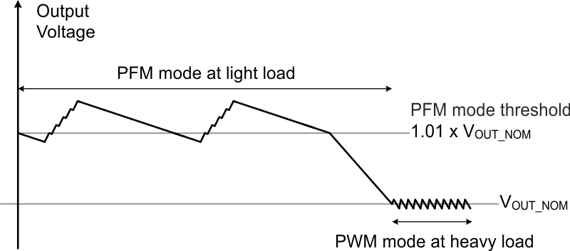 Figure 6. Output Voltage in PFM and PWM Mode
7.4.2.4 PWM Mode
The step-up converter uses a quasi-constant 1.0-MHz frequency pulse width modulation (PWM) at moderate to heavy load current. Based on the input voltage to output voltage ratio, a circuit predicts the required off-time. At the beginning of the switching cycle, the NMOS switching FET is turned on. The input voltage is applied across the inductor and the inductor current ramps up. In this phase, the output capacitor is discharged by the load current. When the inductor current hits the current threshold that is set by the output of the error amplifier, the PWM switch is turned off, and the power diode is forward-biased. The inductor transfers its stored energy to charge the output capacitor and supply the load. When the off-time is expired, the next switching cycle starts again. The error amplifier compares the FB pin voltage with an internal reference voltage, and its output determines the inductor peak current.
7.4.2.5 Constant-Current Step-Up Mode Operation
With pin BM = high the converter can regulate to a constant output current. The internal reference voltage is therefore reduced to 200mV. In order to regulate a constant output current, a sense resistor has to be connected between pin FB and GND, see Figure 7. The device features in this operation mode a PWM to analog converter at pin EN2/PWM. The internal reference voltage is scaled according to the duty cycle of the PWM signal applied to pin EN2/PWM, see Figure 8. When the pin EN2/PWM is pulled low longer than tDim_OFF max, the step-up converter enters shutdown mode. The constant output current IOUT2 can be calculated according equations Equation 1 and Equation 2.
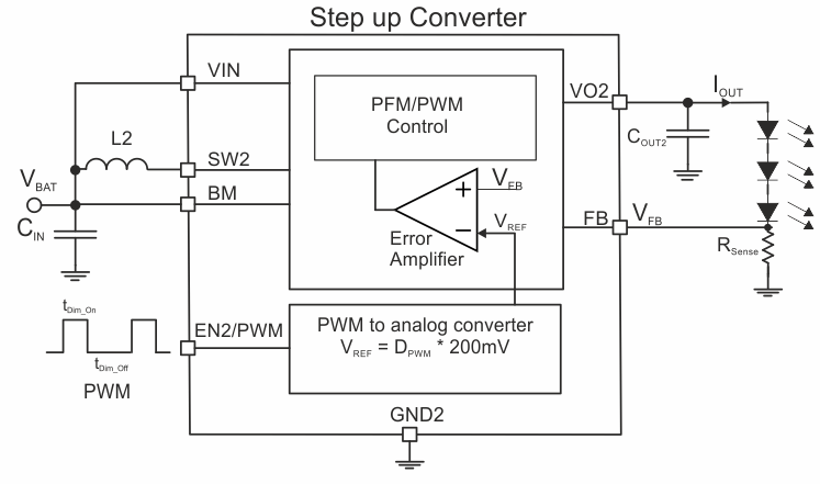 Figure 7. Step-Up Converter in Constant-Current Operation Mode
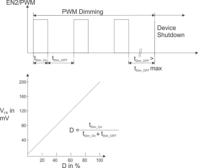 Figure 8. EN2/PWM Pin Function


7.4.2.6 Constant-Voltage Step-Up Mode Operation
With pin BM = low the converter operates as a constant output voltage step-up converter. The internal reference voltage is set to 795 mV. A feedback resistor divider need to be connected between VOUT, FB and GND with its tap point connected to FB pin. The device provides a fixed set 12 V output voltage if the FB pin is connected to VIN. In this case no external resistor divider network is needed.