ZHCSHW0F December 2008 – May 2019 TPS61500
PRODUCTION DATA.
- 1 特性
- 2 应用
- 3 说明
- 4 修订历史记录
- 5 Pin Configuration and Functions
- 6 Specifications
- 7 Detailed Description
-
8 Application and Implementation
- 8.1 Application Information
- 8.2
Typical Applications
- 8.2.1
Analog Dimming Method
- 8.2.1.1 Design Requirements
- 8.2.1.2
Detailed Design Procedure
- 8.2.1.2.1 Programming the Overvoltage Protection
- 8.2.1.2.2 Programming the LED Current
- 8.2.1.2.3 Implementing Dimming
- 8.2.1.2.4 Computing the Maximum Output Current
- 8.2.1.2.5 Selecting the Inductor
- 8.2.1.2.6 Selecting the Schottky Diode
- 8.2.1.2.7 Selecting the Compensation Capacitor and Resistor
- 8.2.1.2.8 Selecting the Input and Output Capacitor
- 8.2.1.3 Application Curves
- 8.2.2 Pure PWM Dimming Method
- 8.2.1
Analog Dimming Method
- 9 Power Supply Recommendations
- 10Layout
- 11器件和文档支持
- 12机械、封装和可订购信息
6.6 Typical Characteristics
Table 1. Table of Graphs
| FIGURE | ||
|---|---|---|
| Efficiency | VIN = 5 V, 4 LEDs, 8 LEDs, 10 LEDs | Figure 1 |
| Efficiency | VIN = 5 V, 12 V; VOUT = 8 LEDs | Figure 2 |
| FB voltage accuracy | vs Temperature | Figure 3 |
| Switch current limit | vs Duty cycle | Figure 4 |
| Switch current limit | vs Temperature | Figure 5 |
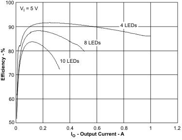 Figure 1. Efficiency
 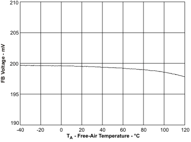 Figure 3. FB Voltage Accuracy
 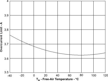 Figure 5. Switch Current Limit
 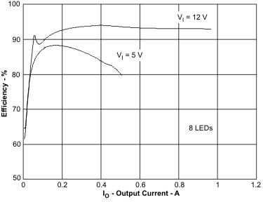 Figure 2. Efficiency
 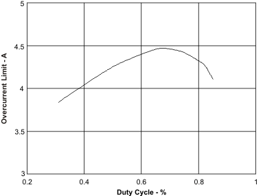 Figure 4. Switch Current Limit