ZHCSJH2E November   2007  – April 2019 TPS61165

PRODUCTION DATA.  

  1. 特性
  2. 应用
  3. 说明
    1.     Device Images
      1.      典型应用
  4. 修订历史记录
  5. Device Options
  6. Pin Configuration and Functions
    1.     Pin Functions
  7. Specifications
    1. 7.1 Absolute Maximum Ratings
    2. 7.2 Recommended Operating Conditions
    3. 7.3 Thermal Information
    4. 7.4 Electrical Characteristics
    5. 7.5 Timing Requirements
    6. 7.6 Typical Characteristics
  8. Detailed Description
    1. 8.1 Overview
    2. 8.2 Functional Block Diagram
    3. 8.3 Feature Description
      1. 8.3.1 Soft Start-Up
      2. 8.3.2 Open LED Protection
      3. 8.3.3 Undervoltage Lockout
      4. 8.3.4 Thermal Shutdown
    4. 8.4 Device Functional Modes
      1. 8.4.1 Shutdown
  9. Application and Implementation
    1. 9.1 Application Information
      1. 9.1.1 Maximum Output Current
      2. 9.1.2 Inductor Selection
      3. 9.1.3 Schottky Diode Selection
      4. 9.1.4 Compensation Capacitor Selection
      5. 9.1.5 Input and Output Capacitor Selection
    2. 9.2 Typical Applications
      1. 9.2.1 TPS61165 Typical Application
        1. 9.2.1.1 Design Requirements
        2. 9.2.1.2 Detailed Design Procedure
          1. 9.2.1.2.1 LED Brightness Dimming Mode Selection
          2. 9.2.1.2.2 PWM Brightness Dimming
          3. 9.2.1.2.3 Digital One-Wire Brightness Dimming
          4. 9.2.1.2.4 EasyScale: One-Wire Digital Dimming
          5. 9.2.1.2.5 Current Program
        3. 9.2.1.3 Application Curves
      2. 9.2.2 Additional Application Circuits
    3. 9.3 Do's and Don'ts
  10. 10Power Supply Recommendations
  11. 11Layout
    1. 11.1 Layout Guidelines
    2. 11.2 Layout Example
    3. 11.3 Thermal Considerations
  12. 12器件和文档支持
    1. 12.1 器件支持
      1. 12.1.1 第三方产品免责声明
    2. 12.2 文档支持
      1. 12.2.1 相关文档
    3. 12.3 社区资源
    4. 12.4 商标
    5. 12.5 静电放电警告
    6. 12.6 术语表
  13. 13机械、封装和可订购信息

封装选项

机械数据 (封装 | 引脚)
散热焊盘机械数据 (封装 | 引脚)
订购信息

Pin Configuration and Functions

DRV Package
6-Pin WSON With Thermal Pad
Top View
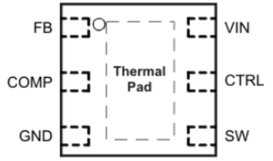
TPS61165 pin1_slvs790.gif
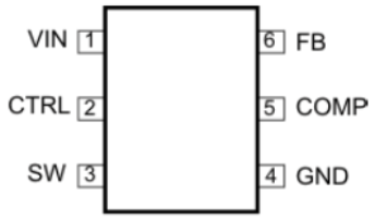
DBV Package
6-Pin SOT-23
Top View
TPS61165 pin2_slvs790.gif

Pin Functions

PIN TYPE DESCRIPTION
NAME WSON
NO.
SOT-23
NO.
CTRL 5 2 I Control pin of the boost converter. It is a multifunctional pin which can be used for enable control, PWM and digital dimming.
COMP 2 5 O Output of the transconductance error amplifier. Connect an external capacitor to this pin to compensate the converter.
FB 1 6 I Feedback pin for current. Connect the sense resistor from FB to GND.
GND 3 4 O Ground
SW 4 3 I This is the switching node of the device. Connect the switched side of the inductor to SW. This pin is also used to sense the output voltage for open LED protection.
VIN 6 1 I The input supply pin for the IC. Connect VIN to a supply voltage between 3 V and 18 V.
Thermal Pad The thermal pad must be soldered to the analog ground plane. If possible, use thermal via to connect to ground plane for ideal power dissipation.