SLVS888C December   2008  – October 2015 TPS60150

PRODUCTION DATA.  

  1. Features
  2. Applications
  3. Description
  4. Revision History
  5. Pin Configuration and Functions
  6. Specifications
    1. 6.1 Absolute Maximum Ratings
    2. 6.2 ESD Ratings
    3. 6.3 Recommended Operating Conditions
    4. 6.4 Thermal Information
    5. 6.5 Electrical Characteristics
    6. 6.6 Typical Characteristics
  7. Detailed Description
    1. 7.1 Overview
    2. 7.2 Functional Block Diagram
    3. 7.3 Feature Description
      1. 7.3.1 Enable
      2. 7.3.2 Undervoltage Lockout
      3. 7.3.3 Thermal Shutdown Protection
    4. 7.4 Device Functional Modes
      1. 7.4.1 Soft Start
      2. 7.4.2 Normal Mode and Skip Mode Operation
      3. 7.4.3 Short Circuit Protection
  8. Application and Implementation
    1. 8.1 Application Information
    2. 8.2 Typical Application
      1. 8.2.1 USB On the Go Circuitry
        1. 8.2.1.1 Design Requirements
        2. 8.2.1.2 Detailed Design Procedure
          1. 8.2.1.2.1 Capacitor Selection
        3. 8.2.1.3 Application Curves
      2. 8.2.2 System Example
  9. Power Supply Recommendations
  10. 10Layout
    1. 10.1 Layout Guidelines
    2. 10.2 Layout Example
  11. 11Device and Documentation Support
    1. 11.1 Community Resources
    2. 11.2 Trademarks
    3. 11.3 Electrostatic Discharge Caution
    4. 11.4 Glossary
  12. 12Mechanical, Packaging, and Orderable Information

封装选项

机械数据 (封装 | 引脚)
散热焊盘机械数据 (封装 | 引脚)
订购信息

10 Layout

10.1 Layout Guidelines

Large transient currents flow in the VIN, VOUT, and GND traces. To minimize both input and output ripple, keep the capacitors as close as possible to the regulator using short, direct circuit traces.

10.2 Layout Example
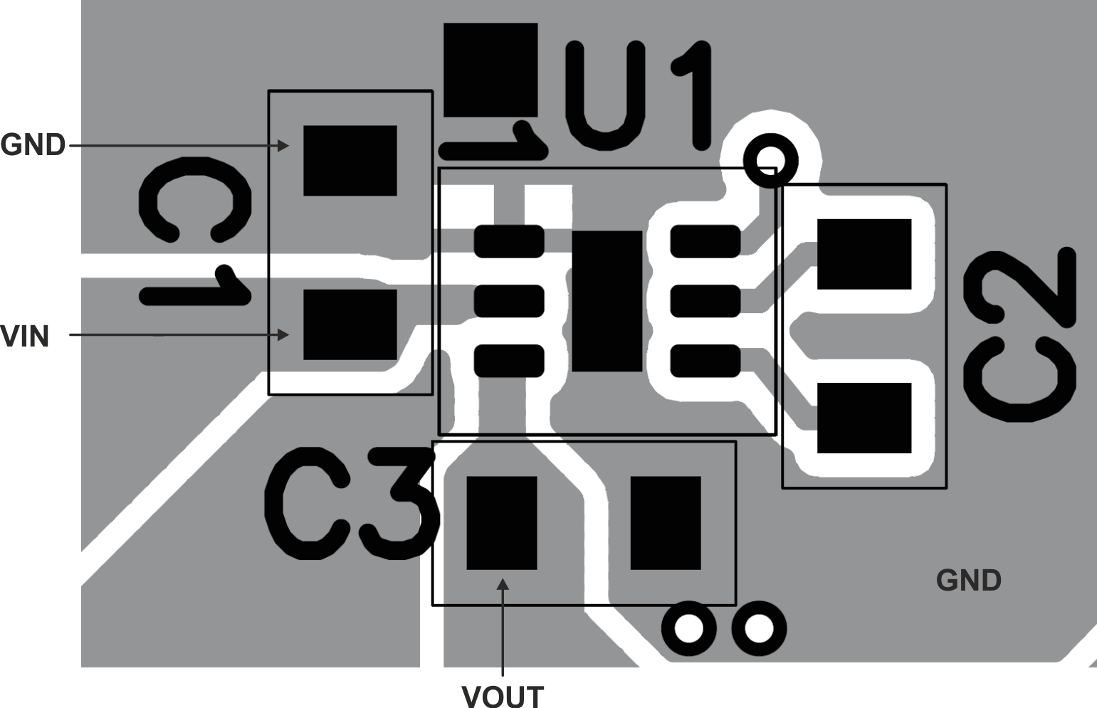
TPS60150 pcb_lvs888_update.gif Figure 24. Recommended PCB Layout