SLVS888C December 2008 – October 2015 TPS60150
PRODUCTION DATA.
8 Application and Implementation
NOTE
Information in the following applications sections is not part of the TI component specification, and TI does not warrant its accuracy or completeness. TI’s customers are responsible for determining suitability of components for their purposes. Customers should validate and test their design implementation to confirm system functionality.
8.1 Application Information
Most of today’s battery-powered portable electronics allow and/or require data transfer with a PC. One of the fastest data transfer protocols is through USB On-the-Go (OTG). As Figure 7 shows, the USB OTG circuitry in the portable device requires a 5-V power rail and up to 140 mA of current. The TPS60150 device may be used to provide a 5-V power rail in a battery powered system.
8.2 Typical Application
8.2.1 USB On the Go Circuitry
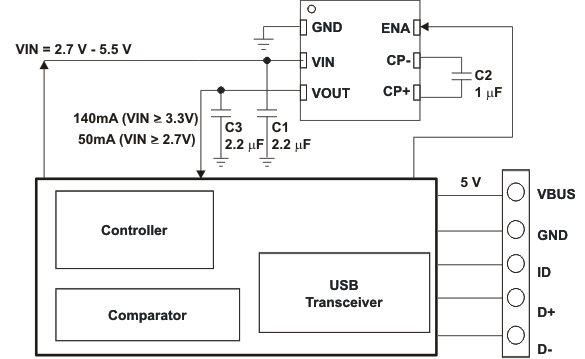 Figure 7. Application Circuit for OTG System
8.2.1.1 Design Requirements
The design guideline provides a component selection to operate the device within the Recommended Operating Conditions.
8.2.1.2 Detailed Design Procedure
8.2.1.2.1 Capacitor Selection
For minimum output voltage ripple, the output capacitor (COUT) should be a surface-mount ceramic capacitor. Tantalum capacitors generally have a higher effective series resistance (ESR) and may contribute to higher output voltage ripple. Leaded capacitors also increase ripple due to the higher inductance of the package itself. To achieve the best operation with low input voltage and high load current, the input and flying capacitors (CIN and CF, respectively) should also be surface-mount ceramic types.
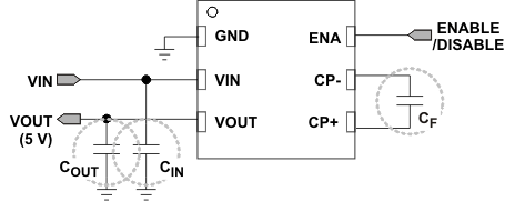 Figure 8. Capacitors
Generally, CFLY can be calculated using Equation 2.

Both equation should be same, 

If ILOAD = 140 mA, f = 1.5 MHZ, and ΔVCFLY = 100 mV, the minimum value of the flying capacitor should be 1 μF.
Output capacitance, COUT, is also strongly related to output ripple voltage and loop stability,

The minimum output capacitance for all output levels is 2.2 μF due to control stability. Larger ceramic capacitors or low ESR capacitors can be used to lower the output ripple voltage.
Table 1. Suggested Capacitors (Input, Output, and Flying Capacitor)
| VALUE | DIELECTRIC MATERIAL | PACKAGE SIZE | RATED VOLTAGE |
|---|---|---|---|
| 4.7 μF | X5R or X7R | 0603 | 10 V |
| 2.2 μF | X5R or X7R | 0603 | 10 V |
The efficiency of the charge pump regulator varies with the output voltage, the applied input voltage and the load current.
Use Equation 5 and Equation 6 to calculate the approximate efficiency in normal operating mode is given by:


8.2.1.3 Application Curves
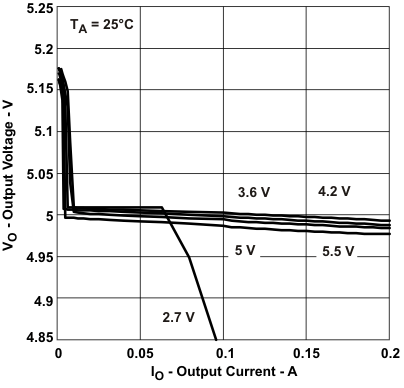 Figure 9. Output Voltage vs Output Current
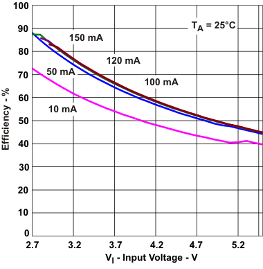 Figure 11. Efficiency vs Input Voltage
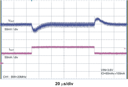 Figure 13. Load Transient Response
 VIN = 3.6 V, IO = 60 mA to 100 mA
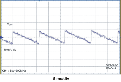 Figure 15. Output Ripple Voltage (Skip Mode)
 VIN = 3.6 V, IO = 0 mA
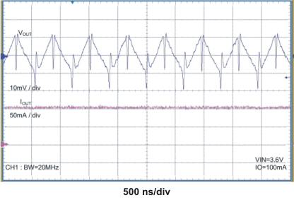 Figure 17. Output Ripple (Normal Mode)
 VIN = 3.6 V, IO = 100 mA
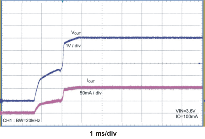 Figure 19. Power On
 VIN = 3.6 V, IO = 100 mA
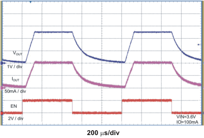 Figure 21. Enable / Disable
 VIN = 3.6 V, IO = 100 mA
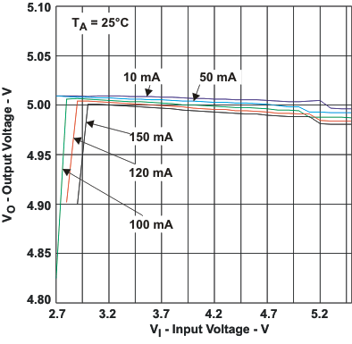 Figure 10. Output Voltage vs Input Voltage
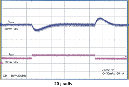 Figure 12. Load Transient Response
 VIN = 2.7 V, IO = 30 mA to 50 mA
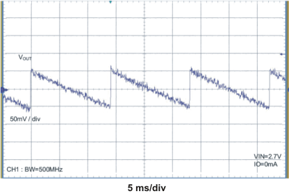 Figure 14. Output Ripple Voltage (Skip Mode)
VIN = 2.7 V, IO = 0 mA
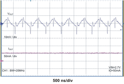 Figure 16. Output Ripple Voltage (Normal Mode)
 VIN = 2.7 V, IO = 50 mA
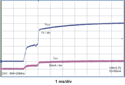 Figure 18. Power On
 VIN = 2.7 V, IO = 50 mA
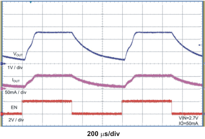 Figure 20. Enable / Disable
VIN = 2.7 V, IO = 50 mA
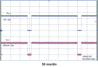 Figure 22. Thermal Shutdown Operation
 VIN = 5.5 V, RLOAD= 20 Ω
8.2.2 System Example
Low-cost portable electronics with small LCD displays require a low-cost solution for providing the WLED backlight. As shown in Figure 23, the TPS60150 device can also be used to drive several WLEDs in parallel, with the help of ballast resistors.
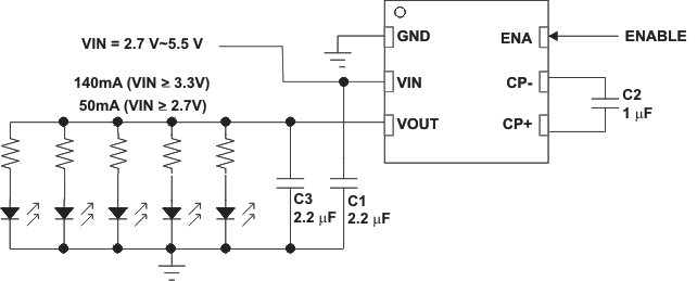 Figure 23. Application Circuit for Driving White LEDs