SLVS888C December 2008 – October 2015 TPS60150
PRODUCTION DATA.
7 Detailed Description
7.1 Overview
The TPS60150 regulated charge pump provides a regulated output voltage for various input voltages. The TPS60150 device regulates the voltage across the flying capacitor to 2.5 V and controls the voltage drop of Q1 and Q2 while a conversion clock with 50% duty cycle drives the FETs.
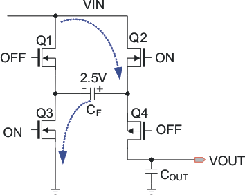 Figure 3. Charging Mode
During the first half cycle, Q2 and Q3 transistors are turned on and flying capacitor, CF, will be charged to 2.5 V ideally.
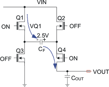 Figure 4. Discharging Mode
During the second half cycle, Q1 and Q4 transistors are turned on. Capacitor CF will then be discharged to output.
Use Equation 1 to calculate the output voltage.

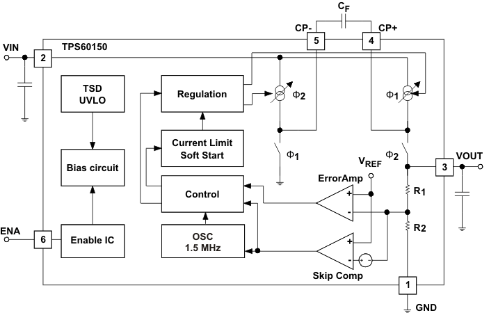
The output voltage is regulated by output feedback and an internally compensated voltage control loop.
7.2 Functional Block Diagram
7.3 Feature Description
7.3.1 Enable
An enable pin on the regulator is used to place the device into an energy-saving shutdown mode. In this mode, the output is disconnected from the input, and the input quiescent current is reduced to 10 μA maximum.
7.3.2 Undervoltage Lockout
When the input voltage drops, the undervoltage lockout prevents misoperation by switching off the device. The converter starts operation again when the input voltage exceeds the threshold, provided the enable pin is high.
7.3.3 Thermal Shutdown Protection
The regulator has thermal shutdown circuitry that protects it from damage caused by overload conditions. The thermal protection circuitry disables the output when the junction temperature reached approximately 160°C, allowing the device to cool. When the junction temperature cools to approximately 140°C, the output circuitry is automatically reenabled. Continuously running the regulator into thermal shutdown can degrade reliability. The regulator also provides current limit to protect itself and the load.
7.4 Device Functional Modes
7.4.1 Soft Start
An internal soft start limits the inrush current when the device is being enabled.
7.4.2 Normal Mode and Skip Mode Operation
The TPS60150 device has skip mode operation as shown in Figure 5. The TPS60150 device enters skip mode if the output voltage reaches 5 V +0.1 V and the load current is less than 8 mA (typical). In skip mode, the TPS60150 device disables the oscillator and decreases the prebias current of the output stage to reduce the power consumption. Once the output voltage dips less than the threshold voltage of 5 V +0.1 V, the TPS60150 device begins switching to increase output voltage until the output reaches 5 V +0.1 V. When the output voltage dips less than 5 V, the TPS60150 device returns to normal pulse width modulation (PWM) mode; thereby reenabling the oscillator and increasing the prebias current of the output stage to supply output current.
The skip threshold voltage and current depend on input voltage and output current conditions.
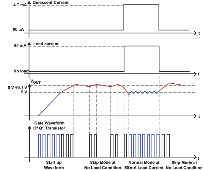 Figure 5. Normal Mode and Skip Mode Operation
7.4.3 Short Circuit Protection
The TPS60150 device has internal short circuit protection to protect the IC when the output is shorted to ground. To avoid damage when output is shorted to ground, the short circuit protection circuitry senses output voltage and clamps the maximum output current to 80 mA (typical).
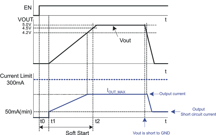 Figure 6. Maximum Output Current Capability and Short Circuit Protection