ZHCSH41A November   2017  – December 2021 TPS55160-Q1 , TPS55162-Q1 , TPS55165-Q1

PRODUCTION DATA  

  1. 特性
  2. 应用
  3. 说明
  4. Revision History
  5. 说明(续)
  6. Pin Configuration and Functions
  7. Specifications
    1. 7.1  Absolute Maximum Ratings
    2. 7.2  ESD Ratings
    3. 7.3  Recommended Operating Conditions
    4. 7.4  Thermal Information
    5. 7.5  Electrical Characteristics — External Components
    6. 7.6  Electrical Characteristics — Supply Voltage (VINP, VINL pins)
    7. 7.7  Electrical Characteristics — Reference Voltage (VOS_FB Pin) and Output Voltage (VOUT Pin)
    8. 7.8  Electrical Characteristics — Buck-Boost
    9. 7.9  Electrical Characteristics — Undervoltage and Overvoltage Lockout
    10. 7.10 Electrical Characteristics — IGN Wakeup
    11. 7.11 Electrical Characteristics — Logic Pins PS, IGN_PWRL, SS_EN
    12. 7.12 Electrical Characteristics – Overtemperature Protection
    13. 7.13 Electrical Characteristics – Power Good
    14. 7.14 Switching Characteristics — Reference Voltage (VOS_FB Pin) and Output Voltage (VOUT Pin)
    15. 7.15 Switching Characteristics — Buck-Boost
    16. 7.16 Switching Characteristics — Undervoltage and Overvoltage Lockout
    17. 7.17 Switching Characteristics — IGN Wakeup
    18. 7.18 Switching Characteristics — Logic Pins PS, IGN_PWRL, SS_EN
    19. 7.19 Switching Characteristics – Power Good
    20. 7.20 Typical Characteristics
  8. Detailed Description
    1. 8.1 Overview
    2. 8.2 Functional Block Diagram
    3. 8.3 Feature Description
      1. 8.3.1 Spread-Spectrum Feature
      2. 8.3.2 Overcurrent Protection
      3. 8.3.3 Overtemperature Protection
      4. 8.3.4 Undervoltage Lockout and Minimum Start-Up Voltage
      5. 8.3.5 Overvoltage Lockout
      6. 8.3.6 VOUT Overvoltage Protection
      7. 8.3.7 Power-Good Pin
    4. 8.4 Device Functional Modes
      1. 8.4.1 State Diagram
      2. 8.4.2 Modes of Operation
        1. 8.4.2.1 Normal Mode
        2. 8.4.2.2 Low-Power Mode
      3. 8.4.3 Power-Up and Power-Down Sequences
      4. 8.4.4 Soft-Start Feature
      5. 8.4.5 Pulldown Resistor on VOUT
      6. 8.4.6 Output Voltage Selection
  9. Application and Implementation
    1. 9.1 Application Information
      1. 9.1.1 Application Circuits for Output Voltage Configurations
    2. 9.2 Typical Application
      1. 9.2.1 Design Requirements
      2. 9.2.2 Detailed Design Procedure
        1. 9.2.2.1 Power-Circuit Selections: CIN, L, COUT
          1. 9.2.2.1.1 Inductor Current in Step-Down Mode
          2. 9.2.2.1.2 Inductor Current in Step-Up Mode
          3. 9.2.2.1.3 Inductor Current in Buck-Boost Overlap Mode
          4. 9.2.2.1.4 Inductor Peak Current
        2. 9.2.2.2 Control-Circuit Selections
          1. 9.2.2.2.1 Bootstrap Capacitors
          2. 9.2.2.2.2 VOUT-Sense Bypass Capacitor
          3. 9.2.2.2.3 VREG Bypass Capacitor
          4. 9.2.2.2.4 PG Pullup Resistor and Delay Time
      3. 9.2.3 Application Curves
  10. 10Power Supply Recommendations
  11. 11Layout
    1. 11.1 Layout Guidelines
    2. 11.2 Layout Example
  12. 12Device and Documentation Support
    1. 12.1 Device Support
      1. 12.1.1 Development Support
    2. 12.2 Documentation Support
      1. 12.2.1 Related Documentation
    3. 12.3 接收文档更新通知
    4. 12.4 支持资源
    5. 12.5 Trademarks
    6. 12.6 Electrostatic Discharge Caution
    7. 12.7 术语表
  13. 13Mechanical, Packaging, and Orderable Information

封装选项

机械数据 (封装 | 引脚)
散热焊盘机械数据 (封装 | 引脚)
订购信息

Power-Up and Power-Down Sequences

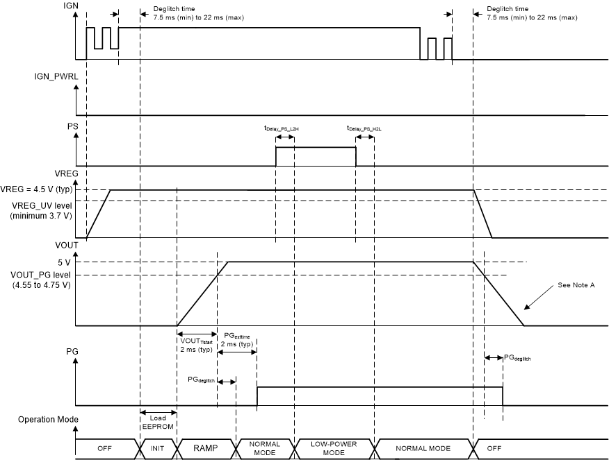
Figure 8-2 shows the power-up and power-down sequence without the usage of the IGN_PWRL pin.
GUID-96B32DDC-38B7-46F8-B063-CF5ABE69C939-low.gif
The actual ramp-down time of the output voltage depends on external load conditions.
Figure 8-2 Power-Up and Power-Down Sequence With Normal Mode and Low-Power Mode, Without Usage of IGN_PWRL

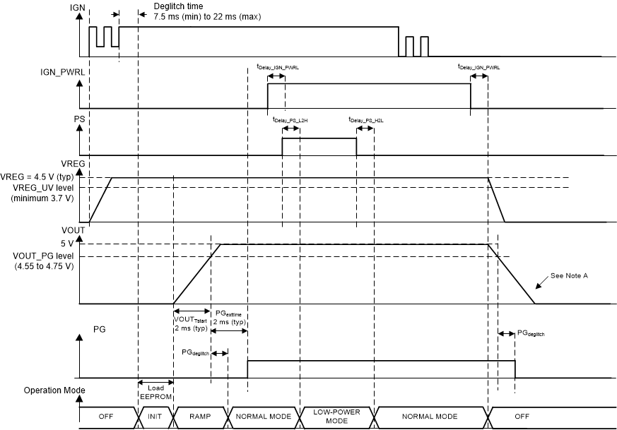
Figure 8-3 shows the power-up and power-down sequence with usage of the IGN_PWRL pin.
GUID-915F6C50-6DDE-487B-A351-C860A2A6413A-low.gif
The actual ramp-down time of the output voltage depends on external load conditions.
Figure 8-3 Power-Up and Power-Down Sequence With Normal Mode and Low-Power Mode, With Usage of IGN_PWRL

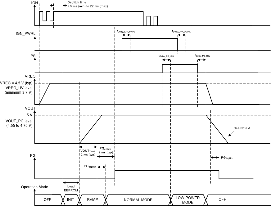
Figure 8-4 shows a power-up and power-down sequence in low-Power mode with the IGN pin low. Figure 8-4 shows that after the device is powered on in the OFF state, the device is in low-power mode when the PS pin is high regardless of what was applied on the IGN and IGN_PWRL input pins.
GUID-E26D29E7-FB21-4578-80AF-B10499BE1F49-low.gif
The actual ramp-down time of the output voltage depends on external load conditions.
Figure 8-4 Power-Up and Power-Down Sequence With Low-Power Mode When IGN and IGN_PWRL are Low (Essentially When the ECU is in Sleep or Standby Mode)

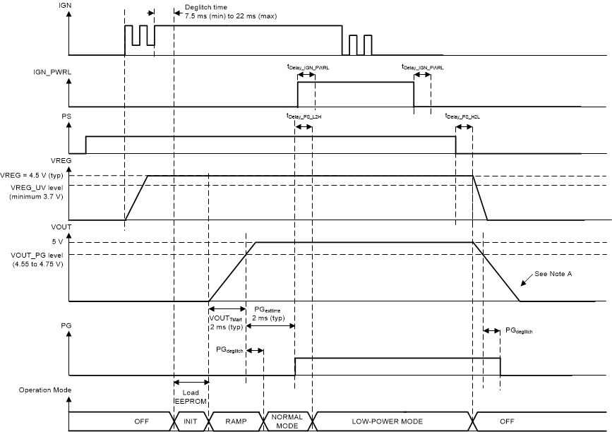
Figure 8-5 shows that when the device starts in the OFF state, the buck-boost converter always enters normal mode first, even when the PS pin was previously set high. The device can only enter low-power mode when the PG output pin is set high. Figure 8-5 also shows that the device does not start-up as long as the IGN pin is low.
GUID-E969A9F7-8490-452E-A970-3C8A6659F506-low.gif
The actual ramp-down time of the output voltage depends on external load conditions.
The buck-boost converter always enters normal mode first after ramp up before it can enter low-power mode.
Figure 8-5 Power-Up Behavior With PS Pin Previously Set High

Figure 8-6 shows that the device only can start-up in the OFF state when the IGN pin is high. Setting the IGN_PWRL pin before the IGN pin is high does not start-up the device. Figure 8-6 also shows that the IGN_PWRL signal is only valid after the PG pin is high and the PGDeglitch time has elapsed.
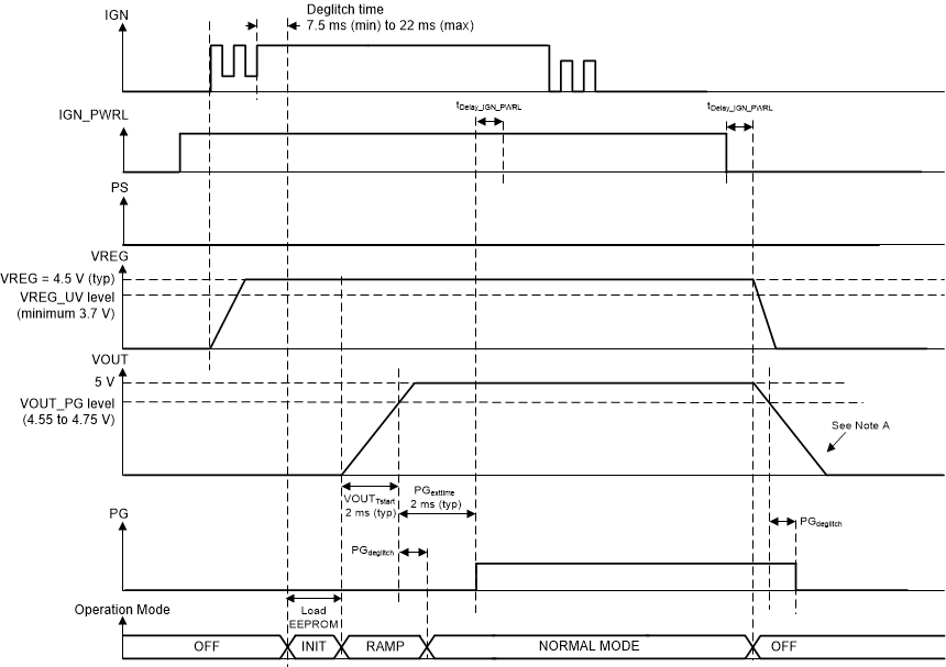
GUID-6A837A2C-E19F-4F8B-ACA2-B7AE48626B6F-low.gif
The actual ramp-down time of the output voltage depends on external load conditions.
The device does not start-up until the IGN pin is high. The IGN power-latch is only be set after the PG pin is high.
Figure 8-6 Power-Up Behavior With IGN_PWRL Set High Prior to High IGN