ZHCSL73B October 2016 – June 2021 TPS54388C-Q1
PRODUCTION DATA
- 1 特性
- 2 应用
- 3 说明
- 4 Revision History
- 5 Pin Configuration and Functions
- 6 Specifications
-
7 Detailed Description
- 7.1 Overview
- 7.2 Functional Block Diagram
- 7.3 Feature Description
- 7.4
Device Functional Modes
- 7.4.1 Adjusting the Output Voltage
- 7.4.2 Enable Functionality and Adjusting Undervoltage Lockout
- 7.4.3 Slow-Start or Tracking Pin
- 7.4.4 Sequencing
- 7.4.5 Constant Switching Frequency and Timing Resistor (RT/CLK Pin)
- 7.4.6 Overcurrent Protection
- 7.4.7 Frequency Shift
- 7.4.8 Reverse Overcurrent Protection
- 7.4.9 Synchronize Using the RT/CLK Pin
- 7.4.10 Power Good (PWRGD Pin)
- 7.4.11 Overvoltage Transient Protection
- 7.4.12 Thermal Shutdown
- 7.4.13 Small-Signal Model for Loop Response
- 7.4.14 Simple Small-Signal Model for Peak-Current-Mode Control
- 7.4.15 Small-Signal Model for Frequency Compensation
-
8 Application and Implementation
- 8.1 Application Information
- 8.2
Typical Application
- 8.2.1 Design Requirements
- 8.2.2
Detailed Design Procedure
- 8.2.2.1 Selecting the Switching Frequency
- 8.2.2.2 Output Inductor Selection
- 8.2.2.3 Output Capacitor
- 8.2.2.4 Input Capacitor
- 8.2.2.5 Slow-Start Capacitor
- 8.2.2.6 Bootstrap Capacitor Selection
- 8.2.2.7 Output-Voltage and Feedback-Resistor Selection
- 8.2.2.8 Compensation
- 8.2.2.9 Power-Dissipation Estimate
- 8.2.3 Application Curves
- 9 Power Supply Recommendations
- 10Layout
- 11Device and Documentation Support
- 12Mechanical, Packaging, and Orderable Information
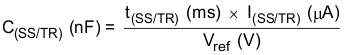
7.4.3 Slow-Start or Tracking Pin
The TPS54388C-Q1 device regulates to the lower of the SS/TR pin and the internal reference voltage. A capacitor on the SS/TR pin to ground implements a slow-start time. The TPS54388C-Q1 device has an internal pullup current source of 2 μA, which charges the external slow-start capacitor. Equation 4 calculates the required slow-start capacitor value, where t(SS/TR) is the desired slow start time in ms, I(SS/TR) is the internal slow start charging current of 2 μA, and Vref is the internal voltage reference of 0.8 V.
If during normal operation, VIN goes below UVLO, the EN pin goes below 1.2 V, or a thermal shutdown event occurs, the TPS54388C-Q1 device stops switching. On VIN going above UVLO, the release or pulling high of EN, or exit from a thermal shutdown, SS/TR discharges to below 60 mV before re-initiation of a power-up sequence. The VSENSE voltage follows the SS/TR pin voltage with a 50-mV offset up to 85% of the internal voltage reference. When the SS/TR voltage is greater than 85% of the internal reference voltage, the offset increases as the effective system reference transitions from the SS/TR voltage to the internal voltage reference.