ZHCSL73B October 2016 – June 2021 TPS54388C-Q1
PRODUCTION DATA
- 1 特性
- 2 应用
- 3 说明
- 4 Revision History
- 5 Pin Configuration and Functions
- 6 Specifications
-
7 Detailed Description
- 7.1 Overview
- 7.2 Functional Block Diagram
- 7.3 Feature Description
- 7.4
Device Functional Modes
- 7.4.1 Adjusting the Output Voltage
- 7.4.2 Enable Functionality and Adjusting Undervoltage Lockout
- 7.4.3 Slow-Start or Tracking Pin
- 7.4.4 Sequencing
- 7.4.5 Constant Switching Frequency and Timing Resistor (RT/CLK Pin)
- 7.4.6 Overcurrent Protection
- 7.4.7 Frequency Shift
- 7.4.8 Reverse Overcurrent Protection
- 7.4.9 Synchronize Using the RT/CLK Pin
- 7.4.10 Power Good (PWRGD Pin)
- 7.4.11 Overvoltage Transient Protection
- 7.4.12 Thermal Shutdown
- 7.4.13 Small-Signal Model for Loop Response
- 7.4.14 Simple Small-Signal Model for Peak-Current-Mode Control
- 7.4.15 Small-Signal Model for Frequency Compensation
-
8 Application and Implementation
- 8.1 Application Information
- 8.2
Typical Application
- 8.2.1 Design Requirements
- 8.2.2
Detailed Design Procedure
- 8.2.2.1 Selecting the Switching Frequency
- 8.2.2.2 Output Inductor Selection
- 8.2.2.3 Output Capacitor
- 8.2.2.4 Input Capacitor
- 8.2.2.5 Slow-Start Capacitor
- 8.2.2.6 Bootstrap Capacitor Selection
- 8.2.2.7 Output-Voltage and Feedback-Resistor Selection
- 8.2.2.8 Compensation
- 8.2.2.9 Power-Dissipation Estimate
- 8.2.3 Application Curves
- 9 Power Supply Recommendations
- 10Layout
- 11Device and Documentation Support
- 12Mechanical, Packaging, and Orderable Information
7.4.4 Sequencing
One can implement many of the common power-supply sequencing methods using the SS/TR, EN, and PWRGD pins. Implementation of the sequential method uses an open-drain or open-collector output of the power-on-reset pin of another device. Figure 7-3 shows the sequential method. Couple the power-good to the EN pin on the TPS54388C-Q1 device to enable the second power supply once the primary supply reaches regulation.
One can accomplish ratiometric start-up by connecting the SS/TR pins together. The regulator outputs ramp up and reach regulation at the same time. When calculating the slow-start time, double the pullup current source in Equation 4. Figure 7-5 shows the ratiometric method.
 Figure 7-3 Sequential Start-Up Sequence
 Figure 7-4 Sequential Start-Up Using EN and PWRGD
 Figure 7-5 Schematic for Ratiometric Start-Up Sequence
 Leading VO(2)") Figure 7-6 Ratiometric Start-Up With VO(1) Leading VO(2)
Figure 7-6 Ratiometric Start-Up With VO(1) Leading VO(2)One can implement ratiometric and simultaneous power-supply sequencing by connecting the resistor network of R1 and R2 shown in Figure 7-7 to the output of the power supply that requires tracking, or to another voltage reference source. Using Equation 5 and Equation 6, one can calculate the tracking resistors to initiate VO(2) slightly before, after, or at the same time as VO(1). VO(1) – VO(2) is 0 V for simultaneous sequencing. Including V(ssoffset) and I(SS/TR) as variables in the equations minimizes the effect of the inherent SS/TR-to-VSENSE offset (V(ssoffset)) in the slow-start circuit and the offset created by the pullup current source (I(ss)) and tracking resistors. Because the SS/TR pin requires pulling below 60 mV before starting after an EN, UVLO, or thermal-shutdown fault, select the tracking resistors carefully to ensure the device can restart after a fault. Make sure the calculated R1 value from Equation 5 is greater than the value calculated in Equation 7 to ensure the device can recover from a fault. As the SS/TR voltage becomes more than 85% of the nominal reference voltage, V(ssoffset) becomes larger as the slow-start circuits gradually hand off the regulation reference to the internal voltage reference. The SS/TR pin voltage must be greater than 1.1 V for a complete handoff to the internal voltage reference as shown in Figure 7-6.
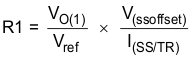
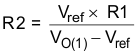

 Figure 7-7 Ratiometric and Simultaneous Start-Up Sequence
 Figure 7-8 Ratiometric Start-Up Using Coupled SS/TR Pins