SLVS932F May 2009 – November 2014 TPS54325
PRODUCTION DATA.
- 1 Features
- 2 Applications
- 3 Description
- 4 Simplified Schematic
- 5 Revision History
- 6 Pin Configuration and Functions
- 7 Specifications
- 8 Detailed Description
- 9 Application and Implementation
- 10Power Supply Recommendations
- 11Layout
- 12Device and Documentation Support
- 13Mechanical, Packaging, and Orderable Information
6 Pin Configuration and Functions
14-Pin
PWP PACKAGE
Top View
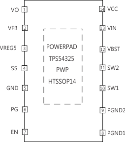
Pin Functions
| PIN | I/O | DESCRIPTION | |
|---|---|---|---|
| NAME | NO. | ||
| VO | 1 | I | Connect to output of converter. This terminal is used for On-Time Adjustment. |
| VFB | 2 | I | Converter feedback input. Connect with feedback resistor divider. |
| VREG5 | 3 | O | 5.5 V power supply output. A capacitor (typical 1μF) should be connected to GND. |
| SS | 4 | I | Soft-start control. A external capacitor should be connected to GND. |
| GND | 5 | –– | Signal ground pin |
| PG | 6 | O | Open drain power good output |
| EN | 7 | I | Enable control input |
| PGND1, PGND2 | 8, 9 | –– | Ground returns for low-side MOSFET. Also serve as inputs of current comparators. Connect PGND and GND strongly together near the IC. |
| SW1, SW2 | 10, 11 | O | Switch node connection between high-side NFET and low-side NFET. Also serve as inputs to current comparators. |
| VBST | 12 | O | Supply input for high-side NFET gate driver (boost terminal). Connect capacitor from this pin to respective SW1, SW2 terminals. An internal PN diode is connected between VREG5 to VBST pin. |
| VIN | 13 | I | Power input and connected to high side NFET drain |
| VCC | 14 | I | Supply input for 5 V internal linear regulator for the control circuitry |
| PowerPAD™ | –– | –– | Thermal pad of the package. Must be soldered to achieve appropriate dissipation. Should be connected to PGND. |