SLVS932F May 2009 – November 2014 TPS54325
PRODUCTION DATA.
- 1 Features
- 2 Applications
- 3 Description
- 4 Simplified Schematic
- 5 Revision History
- 6 Pin Configuration and Functions
- 7 Specifications
- 8 Detailed Description
- 9 Application and Implementation
- 10Power Supply Recommendations
- 11Layout
- 12Device and Documentation Support
- 13Mechanical, Packaging, and Orderable Information
9 Application and Implementation
NOTE
Information in the following applications sections is not part of the TI component specification, and TI does not warrant its accuracy or completeness. TI’s customers are responsible for determining suitability of components for their purposes. Customers should validate and test their design implementation to confirm system functionality.
9.1 Application Information
The TPS54325 device is typically used as a step-down converter, which converts a voltage in the range of 4.5 V to 18 V to a lower voltage. WEBENCH software is available to aid in the design and analysis of circuits.
9.2 Typical Application
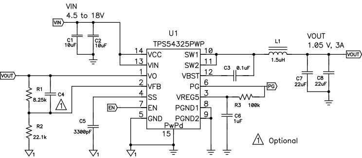 Figure 4. Schematic Diagram for Design Example
9.2.1 Design Requirements
To begin the design process, know the application parameters listed in Table 1:
Table 1. Application Parameters
| PARAMETER | CONDITIONS | MIN | TYP | MAX | UNIT |
|---|---|---|---|---|---|
| Input voltage | 5 | 17 | V | ||
| Output voltage | 1.05 | V | |||
| Operating frequency | VI = 12 V, Io = 1 A | 700 | kHz | ||
| Output current | 0 | 3 | A | ||
| Output ripple voltage | VI = 12 V, Iout = 3 A | 9 | mVpp | ||
| Efficiency | VI = 12 V, Vout = 3.3 V, Iout = 1.2 A | 91% |
9.2.2 Detailed Design Procedure
9.2.2.1 Output Voltage Resistors Selection
The output voltage is set with a resistor divider from the output node to the VFB pin. It is recommended to use 1% tolerance or better divider resistors. Start by using Equation 2 and Equation 3 to calculate VOUT.
To improve efficiency at very light loads consider using larger value resistors, too high of resistance will be more susceptible to noise and voltage errors from the VFB input current will be more noticeable.
For output voltage from 0.76 V to 2.5 V:
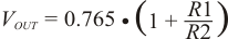
For output voltage over 2.5 V:
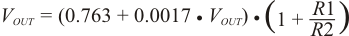
where
- VOUT_SET = Target VOUT voltage
9.2.2.2 Output Filter Selection
The output filter used with the TPS54325 is an LC circuit. This LC filter has double pole at:
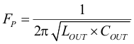
At low frequencies, the overall loop gain is set by the output set-point resistor divider network and the internal gain of the TPS54325. The low frequency phase is 180 degrees. At the output filter pole frequency, the gain rolls off at a -40 dB per decade rate and the phase drops rapidly. D-CAP2 introduces a high frequency zero that reduces the gain roll off to -20 dB per decade and increases the phase to 90 degrees one decade above the zero frequency. The inductor and capacitor selected for the output filter must be selected so that the double pole of Equation 4 is located below the high frequency zero but close enough that the phase boost provided be the high frequency zero provides adequate phase margin for a stable circuit. To meet this requirement use the values recommended in Table 2.
Table 2. Recommended Component Values
| OUTPUT VOLTAGE (V) | R1 (kΩ) | R2 (kΩ) | C4 (pF)(1) | L1 (µH) | C8 + C9 (µF) |
|---|---|---|---|---|---|
| 1 | 6.81 | 22.1 | 1.5 | 22 - 68 | |
| 1.05 | 8.25 | 22.1 | 1.5 | 22 - 68 | |
| 1.2 | 12.7 | 22.1 | 1.5 | 22 - 68 | |
| 1.8 | 30.1 | 22.1 | 10 - 22 | 2.2 | 22 - 68 |
| 2.5 | 49.9 | 22.1 | 10 - 22 | 2.2 | 22 - 68 |
| 3.3 | 73.2 | 22.1 | 10 - 22 | 2.2 | 22 - 68 |
| 5 | 121 | 22.1 | 10 - 22 | 3.3 | 22 - 68 |
For higher output voltages at or above 1.8 V, additional phase boost can be achieved by adding a feed forward capacitor (C4) in parallel with R1.
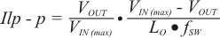
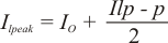
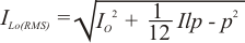
The inductor peak-to-peak ripple current, peak current and RMS current are calculated using Equation 5, Equation 6 and Equation 7. The inductor saturation current rating must be greater than the calculated peak current and the RMS or heating current rating must be greater than the calculated RMS current.
Use 700 kHz for fSW. Make sure the chosen inductor is rated for the peak current of Equation 6 and the RMS current of Equation 7.
For this design example, the calculated peak current is 3.47 A and the calculated RMS current is 3.01 A. The inductor used is a TDK SPM6530-1R5M100 with a peak current rating of 11.5 A and an RMS current rating of 11 A.
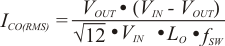
The capacitor value and ESR determines the amount of output voltage ripple. The TPS54325 is intended for use with ceramic or other low ESR capacitors. Recommended values range from 22 µF to 68 µF. Use Equation 8 to determine the required RMS current rating for the output capacitor.
For this design two TDK C3216X5R0J226M 22-µF output capacitors are used. The typical ESR is 2 mΩ each. The calculated RMS current is 0.271 A and each output capacitor is rated for 4 A.
9.2.2.3 Input Capacitor Selection
The TPS54325 requires an input decoupling capacitor, and a bulk capacitor is needed depending on the application. A ceramic capacitor over 10-mF is recommended for the decoupling capacitor. An additional 0.1-µF capacitor from pin 14 to ground is recommended to improve the stability of the over-current limit function. The capacitor voltage rating needs to be greater than the maximum input voltage.
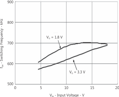
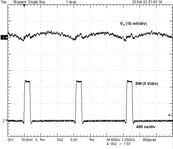
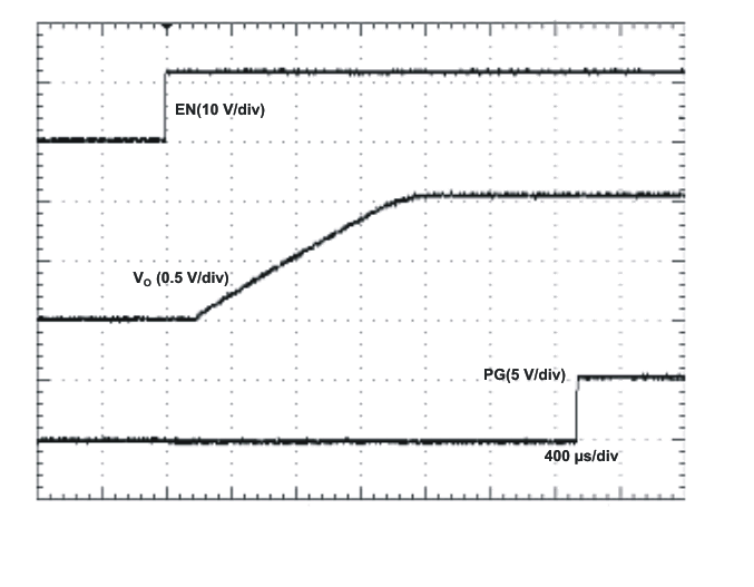
9.2.3 Application Curves
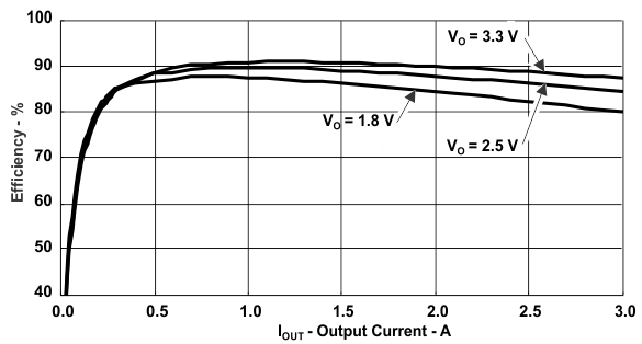
VO = 3.3 V, 2.5 V, and 1.8 V
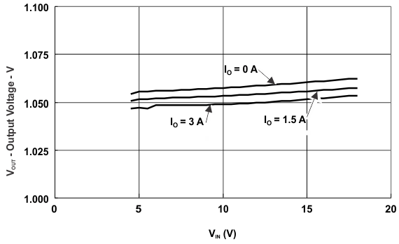
1.05-V Output Voltage vs Input Voltage
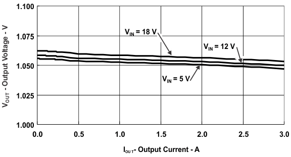
1.05-V Output Voltage vs Output Current