ZHCSQS6C November 2007 – January 2024 TPS5420-Q1
PRODUCTION DATA
- 1
- 1特性
- 2应用
- 3说明
- 4静电放电警告
- 5Ordering Information
- 6Pin Assignments
- 7Specifications
-
8Application Information
- 8.1 Functional Block Diagram
- 8.2
Detailed Description
- 8.2.1 Oscillator Frequency
- 8.2.2 Voltage Reference
- 8.2.3 Enable (ENA) and Internal Slow Start
- 8.2.4 Undervoltage Lockout (UVLO)
- 8.2.5 Boost Capacitor (BOOT)
- 8.2.6 Output Feedback (VSENSE)
- 8.2.7 Internal Compensation
- 8.2.8 Voltage Feed Forward
- 8.2.9 Pulse-Width-Modulation (PWM) Control
- 8.2.10 Overcurrent Limiting
- 8.2.11 Overvoltage Protection (OVP)
- 8.2.12 Thermal Shutdown
- 8.2.13 PCB Layout
- 8.2.14 Application Circuits
- 8.2.15
Design Procedure
- 8.2.15.1 Design Parameters
- 8.2.15.2 Switching Frequency
- 8.2.15.3 Input Capacitors
- 8.2.15.4 Output Filter Components
- 8.2.15.5 Output Voltage Setpoint
- 8.2.15.6 Boot Capacitor
- 8.2.15.7 Catch Diode
- 8.2.15.8 Additional Circuits
- 8.2.15.9 Circuit Using Ceramic Output Filter Capacitors
- 8.2.15.10 Output Filter Component Selection
- 8.2.15.11 External Compensation Network
- 8.3 Advanced Information
- 8.4 Performance Graphs
- 9Revision History
8.2.15.4.1 Inductor Selection
To calculate the minimum value of the output inductor, use Equation 4:
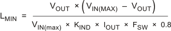
KIND is a coefficient that represents the amount of inductor ripple current relative to the maximum output current. Three things need to be considered when determining the amount of ripple current in the inductor: the peak-to-peak ripple current affects the output ripple voltage amplitude, the ripple current affects the peak switch current, and the amount of ripple current determines at what point the circuit becomes discontinuous. For designs using the TPS5420, KIND of 0.2 to 0.3 yields good results. Low output ripple voltages are obtained when paired with the proper output capacitor, the peak switch current is below the current limit set point, and low load currents can be sourced before discontinuous operation.
For this design example, use KIND = 0.2, and the minimum inductor value is 31 μH. The next highest standard value used in this design is 33 μH.
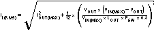
For the output filter inductor, it is important that the RMS current and saturation current ratings not be exceeded. The RMS inductor current is found from Equation 5:
and the peak inductor current is determined from Equation 6:
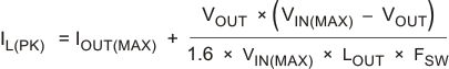
For this design, the RMS inductor current is 2.002 A, and the peak inductor current is 2.16 A. The chosen inductor is a Coilcraft MSS1260-333 type. The nominal inductance is 33 μH. It has a saturation current rating of 2.2 A and a RMS current rating of 2.7 A, which meet the requirements. Inductor values for use with the TPS5420 are in the range of 10 μH to 100 μH.