ZHCSQS6C November 2007 – January 2024 TPS5420-Q1
PRODUCTION DATA
- 1
- 1特性
- 2应用
- 3说明
- 4静电放电警告
- 5Ordering Information
- 6Pin Assignments
- 7Specifications
-
8Application Information
- 8.1 Functional Block Diagram
- 8.2
Detailed Description
- 8.2.1 Oscillator Frequency
- 8.2.2 Voltage Reference
- 8.2.3 Enable (ENA) and Internal Slow Start
- 8.2.4 Undervoltage Lockout (UVLO)
- 8.2.5 Boost Capacitor (BOOT)
- 8.2.6 Output Feedback (VSENSE)
- 8.2.7 Internal Compensation
- 8.2.8 Voltage Feed Forward
- 8.2.9 Pulse-Width-Modulation (PWM) Control
- 8.2.10 Overcurrent Limiting
- 8.2.11 Overvoltage Protection (OVP)
- 8.2.12 Thermal Shutdown
- 8.2.13 PCB Layout
- 8.2.14 Application Circuits
- 8.2.15
Design Procedure
- 8.2.15.1 Design Parameters
- 8.2.15.2 Switching Frequency
- 8.2.15.3 Input Capacitors
- 8.2.15.4 Output Filter Components
- 8.2.15.5 Output Voltage Setpoint
- 8.2.15.6 Boot Capacitor
- 8.2.15.7 Catch Diode
- 8.2.15.8 Additional Circuits
- 8.2.15.9 Circuit Using Ceramic Output Filter Capacitors
- 8.2.15.10 Output Filter Component Selection
- 8.2.15.11 External Compensation Network
- 8.3 Advanced Information
- 8.4 Performance Graphs
- 9Revision History
8.2.15.4.2 Capacitor Selection
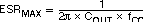
The important design factors for the output capacitor are dc voltage rating, ripple current rating, and equivalent series resistance (ESR). The dc voltage and ripple current ratings cannot be exceeded. The ESR is important because, along with the inductor ripple current, it determines the amount of output ripple voltage. The actual value of the output capacitor is not critical, but some practical limits do exist. Consider the relationship between the desired closed loop crossover frequency of the design and LC corner frequency of the output filter. Due to the design of the internal compensation, it is recommended to keep the closed-loop crossover frequency in the range 3 kHz to 30 kHz, as this frequency range has adequate phase boost to allow for stable operation. For this design example, the intended closed-loop crossover frequency is between 2590 Hz and 24 kHz and below the ESR zero of the output capacitor. Under these conditions, the closed-loop crossover frequency is related to the LC corner frequency as:

and the desired output capacitor value for the output filter to:
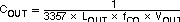
For a desired crossover of 18 kHz and a 33-μH inductor, the calculated value for the output capacitor is 100 μF. The capacitor type should be chosen so that the ESR zero is above the loop crossover. The maximum ESR is: