ZHCSE85A October 2015 – February 2024 TPS3710
PRODUCTION DATA
- 1
- 1 特性
- 2 应用
- 3 说明
- 4 Pin Configuration and Functions
- 5 Specifications
- 6 Detailed Description
- 7 Application and Implementation
- 8 Device and Documentation Support
- 9 Revision History
- 10Mechanical, Packaging, and Orderable Information
7.2.2.1 Resistor Divider Selection
The resistor divider values and target threshold voltage can be calculated by using Equation 1 to determine VMON(UV).
Equation 1. 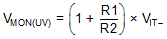
where
- R1 and R2 are the resistor values for the resistor divider on the SENSEx pins
- VMON(UV) is the target voltage at which an undervoltage condition is detected
Choose RTOTAL ( = R1 + R2) so that the current through the divider is approximately 100 times higher than the input current at the SENSE pin. The resistors can have high values to minimize current consumption as a result of low input bias current without adding significant error to the resistive divider. For details on sizing input resistors, refer to application report SLVA450, Optimizing Resistor Dividers at a Comparator Input, available for download from www.ti.com.