ZHCSGZ0B October 2017 – November 2017 TPS23525
PRODUCTION DATA.
- 1 特性
- 2 应用
- 3 说明
- 4 修订历史记录
- 5 Pin Configuration and Functions
- 6 Specifications
- 7 Parameter Measurement Information
- 8 Detailed Description
-
9 Application and Implementation
- 9.1 Application Information
- 9.2
Typical Application
- 9.2.1 Design Requirements
- 9.2.2
Detailed Design Procedure
- 9.2.2.1 Selecting RSNS
- 9.2.2.2 Selecting Soft Start Setting: CSS and CSS,VEE
- 9.2.2.3 Selecting VDS Switch Over Threshold
- 9.2.2.4 Timer Selection
- 9.2.2.5 MOSFET Selection and SOA Checks
- 9.2.2.6 Input Cap, Input TVS, and OR-ing FET selection
- 9.2.2.7 EMI Filter Consideration
- 9.2.2.8 Under Voltage and Over Voltage Settings
- 9.2.2.9 Choosing RVCC and CVCC
- 9.2.2.10 Power Good Interface to Downstream DC/DC
- 9.2.3 Application Curves
- 10Power Supply Recommendations
- 11Layout
- 12器件和文档支持
- 13机械、封装和可订购信息
7.1 Relationship between Sense Voltage, Gate Current, and Timer
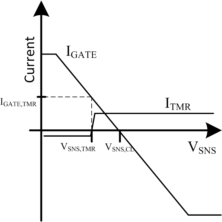
The diagram below illustrates the relationship between the VSNS (voltage across RSNS), Gate current, and the timer operation. The diagram is intended to help explain the various parameters in the electrical characteristic table and is not drawn to scale.
Note that IGATE reduces as the sense voltage approaches the current limit threshold and it equals zero at the current limit regulation point. To ensure that the timer always runs when the IC is in regulation the timer starts at a slightly positive IGATE.
 Figure 7. Relationship Between Timer, Gate Current, and Sense Voltage (VGATE = 5 V)