SLVSDF2A May 2017 – July 2017 TPS22970
PRODUCTION DATA.
- 1 Features
- 2 Applications
- 3 Description
- 4 Revision History
- 5 Pin Configuration and Functions
- 6 Specifications
- 7 Parameter Measurement Information
- 8 Detailed Description
- 9 Application and Implementation
- 10Power Supply Recommendations
- 11Layout
- 12Device and Documentation Support
- 13Mechanical, Packaging, and Orderable Information
8 Detailed Description
8.1 Overview
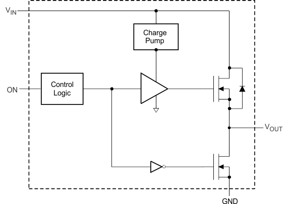
The TPS22970 is a single channel, 4-A load switch in a small, space-saving WCSP-8 package. This device implements a low resistance N-channel MOSFET with a controlled rise time for applications that need to limit the inrush current.
This device is also designed to have very low leakage current during off state, which prevents downstream circuits from pulling high standby current from the supply. Integrated control logic, driver, power supply, and output discharge FET eliminates the need for additional external components, which reduces solution size and bill of materials (BOM) count.
8.2 Functional Block Diagram

8.3 Feature Description
8.3.1 On and Off Control
The ON pin controls the state of the switch. Asserting ON high enables the switch. ON has a low threshold, making it capable of interfacing with low-voltage signals. The ON pin is compatible with standard GPIO logic. It can be used with any microcontroller with 1.2-V, 1.8-V, 2.5-V or 3.3-V GPIOs. This pin does not have an internal bias and must not be left floating for proper functionality.
8.3.2 Quick Output Discharge (QOD)
The TPS22970 includes a QOD feature. When the switch is disabled, a discharge resistor is connected between VOUT and GND. This resistor has a typical value of 150 Ω and prevents the output from floating while the switch is disabled. The QOD pull-down resistance can vary with input voltage and temperature, see Figure 4
8.4 Device Functional Modes
Table 1 lists the functional modes for the TPS22970.
Table 1. Function Table
| TPS22970 | |||
|---|---|---|---|
| ON-Pin | VIN to VOUT | VOUT to GND | |
| Below VIL | OFF | ON | |
| Above VIH | ON | OFF | |