SLVSDF2A May 2017 – July 2017 TPS22970
PRODUCTION DATA.
- 1 Features
- 2 Applications
- 3 Description
- 4 Revision History
- 5 Pin Configuration and Functions
- 6 Specifications
- 7 Parameter Measurement Information
- 8 Detailed Description
- 9 Application and Implementation
- 10Power Supply Recommendations
- 11Layout
- 12Device and Documentation Support
- 13Mechanical, Packaging, and Orderable Information
9 Application and Implementation
NOTE
Information in the following applications sections is not part of the TI component specification, and TI does not warrant its accuracy or completeness. TI’s customers are responsible for determining suitability of components for their purposes. Customers should validate and test their design implementation to confirm system functionality.
9.1 Application Information
9.1.1 Thermal Consideration
It is recommended to limit the junction temperature (TJ) to below 125°C. To calculate the maximum allowable dissipation, PD(max) for a given output current and ambient temperature, use Equation 1 as a guideline.

where
- PD(max) is maximum allowable power dissipation
- TJ(max) is maximum allowable junction temperature
- TA is ambient temperature of the device
- ΘJA is junction to air thermal impedance. See the Thermal Information section. This parameter is highly dependent upon board layout
9.2 Typical Application
 Figure 20. Typical Application Circuit
9.2.1 Design Requirements
For this design example, below, use the input parameters shown in Table 2.
Table 2. Design Parameters
| DESIGN PARAMETER | EXAMPLE VALUE |
|---|---|
| VIN | 0.65 V to 3.6 V |
| ILOAD | 10 mA |
| Load Capacitance (CL) | 800 µF |
| Maximum voltage drop | 1% |
| Maximum Inrush Current | 2.5 A |
9.2.2 Detailed Design Procedure
9.2.2.1 Maximum Voltage Drop and On-Resistance
At 3.6-V input voltage, with a maximum voltage drop tolerance of 1%, the TPS22970 has a typical RON of 4.7 mΩ. The rail is supplying 10 mA of current; the voltage drop for a rail is calculated based on Equation 2 and Equation 3.
The maximum voltage drop is 1% which is 36 mV. The voltage drop caused by the load current across the on resistance is 0.047 mV.
9.2.2.2 Managing Inrush Current
When the switch is enabled, the output capacitors must be charged up from 0 V to VIN. This charge arrives in the form of inrush current. Inrush current may be calculated using Equation 4.

where
- IINRUSH is the Inrush current
- CL is the Load capacitance
- SR is the Output Slew Rate
- VIN is the Input voltage
- tR is the Rise time
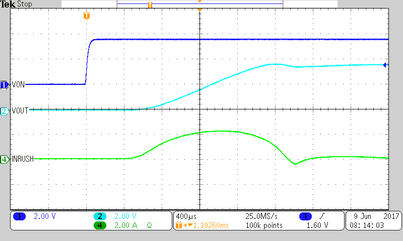
The typical rise time is 985 μs at VIN = 3.6 V. When CL = 800 µF, the expected inrush current limit at the typical rise time is 2.34 A.
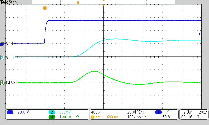
The typical rise time is 320 μs at VIN = 0.65 V. When CL = 800 µF, the expected inrush current limit at the typical rise time is 1.3 A.
9.2.3 Application Curves

| VIN = 3.6 V | VON = 3.6 V | CIN = 1 µF |
| RL = OPEN | TA = 25°C | CL = 800 µF |

| VIN = 0.65 V | VON = 3.6 V | CIN = 1 µF |
| RL = OPEN | TA = 25°C | CL = 800 µF |