ZHCSB59E April 2011 – December 2015 TPS22924B , TPS22924C
PRODUCTION DATA.
- 1 特性
- 2 应用
- 3 说明
- 4 修订历史记录
- 5 Device Comparison Table
- 6 Pin Configuration and Functions
-
7 Specifications
- 7.1 Absolute Maximum Ratings
- 7.2 ESD Ratings
- 7.3 Recommended Operating Conditions
- 7.4 Thermal Information
- 7.5 Electrical Characteristics
- 7.6 Switching Characteristics, VIN = 3.6 V
- 7.7 Switching Characteristics, VIN = 0.9 V
- 7.8 Typical Characteristics
- 7.9 AC Characteristics (TPS22924B)
- 7.10 AC Characteristics (TPS22924C)
- 8 Parameter Measurement Information
- 9 Detailed Description
- 10Application and Implementation
- 11Power Supply Recommendations
- 12Layout
- 13器件和文档支持
- 14机械、封装和可订购信息
封装选项
机械数据 (封装 | 引脚)
散热焊盘机械数据 (封装 | 引脚)
订购信息
12 Layout
12.1 Layout Guidelines
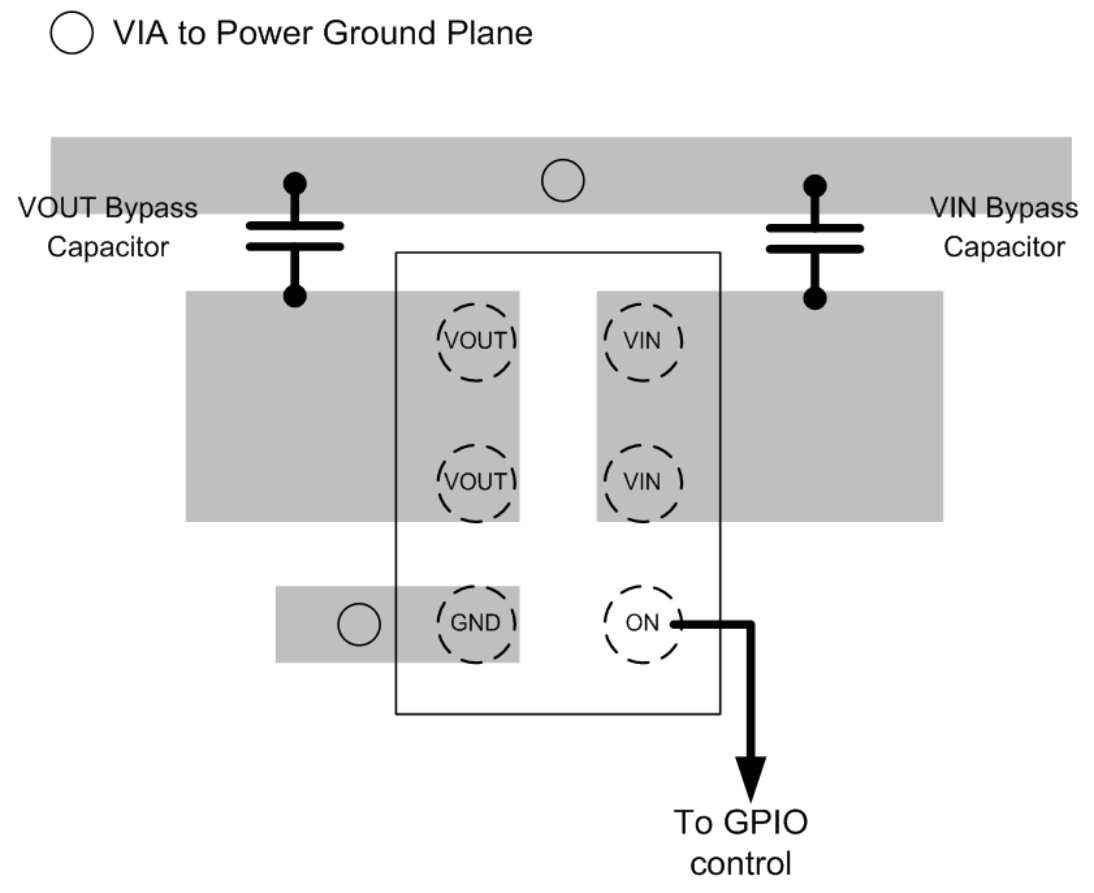
For best performance, all traces should be as short as possible. To be most effective, the input and output capacitors should be placed close to the device to minimize the effects that parasitic trace inductances may have on normal and short-circuit operation. Using wide traces for VIN, VOUT, and GND helps minimize the parasitic electrical effects.
12.2 Layout Example
 Figure 46. TPS22924x Layout Example