ZHCSEG1 December 2015 TPIC2030
PRODUCTION DATA.
- 1 特性
- 2 应用
- 3 说明
- 4 修订历史记录
- 5 说明(续)
- 6 Pin Configuration and Functions
-
7 Specifications
- 7.1 Absolute Maximum Ratings
- 7.2 ESD Ratings
- 7.3 Recommended Operating Conditions
- 7.4 Thermal Information
- 7.5 Electrical Characteristics - Common Part
- 7.6 Electrical Characteristics - Charge Pump Part
- 7.7 Electrical Characteristics - DC-DC Converter
- 7.8 Electrical Characteristics - Spindle Motor Driver Part
- 7.9 Electrical Characteristics - Sled Motor Driver Part
- 7.10 Electrical Characteristics - Focus/ Tilt/Tracking/Driver Part
- 7.11 Electrical Characteristics - Load Driver Part
- 7.12 Electrical Characteristics - Current Switch Part
- 7.13 Electrical Characteristics - LED Switch Part
- 7.14 Electrical Characteristics - Thermometer Part
- 7.15 Electrical Characteristics - Actuator Protection
- 7.16 Electrical Characteristics - Serial Port Voltage Levels
- 7.17 Serial Port I/F Write Timing Requirements
- 7.18 Serial I/F Read Timing Requirements
- 7.19 Typical Characteristics
-
8 Detailed Description
- 8.1 Overview
- 8.2 Functional Block Diagram
- 8.3 Feature Description
- 8.4 Device Functional Modes
- 8.5 Programming
- 8.6
Register Maps
- 8.6.1 Register State Transition
- 8.6.2 DAC Register (12-Bit Write Only)
- 8.6.3 Control Register
- 8.6.4
Detailed Description of Registers
- 8.6.4.1 REG01 12-bit DAC for Tilt (VDAC_MAPSW = 0)
- 8.6.4.2 REG02 12-bit DAC for Focus (VDAC_MAPSW = 0)
- 8.6.4.3 REG03 12-bit DAC for Track (VDAC_MAPSW = 0)
- 8.6.4.4 REG04 10bit DAC for Sled1 (VDAC_MAPSW = 0)
- 8.6.4.5 REG05 10bit DAC for Sled2 (VDAC_MAPSW = 0)
- 8.6.4.6 REG08 12-bit DAC for Spindle (VDAC_MAPSW = 0)
- 8.6.4.7 REG09 12-bit DAC for Load (VDAC_MAPSW = 0)
- 8.6.4.8 REG65 8bit Control Register for FBSVR
- 8.6.4.9 REG6D 8bit Control Register for DCCfg
- 8.6.4.10 REG6E 8bit Control Register for UtilCfg
- 8.6.4.11 REG6F 8bit Control Register for MonitorSet (REG6F)
- 8.6.4.12 REG70 8bit Control Register for DriverEna
- 8.6.4.13 REG71 8bit Control Register for FuncEna
- 8.6.4.14 REG72 8bit Control Register for ACTCfg
- 8.6.4.15 REG73 8bit Control Register for Parm0
- 8.6.4.16 REG74 8bit Control Register for OptSet
- 8.6.4.17 REG76 8bit Control Register for WriteEna
- 8.6.4.18 REG77 8bit Control Register for ClrReg
- 8.6.4.19 REG78 8bit Control Register for ActTemp
- 8.6.4.20 REG79 8bit Control Register for UVLOMon
- 8.6.4.21 REG7A 8bit Control Register for TsdMon
- 8.6.4.22 REG7B 8bit Control Register for ProtMon
- 8.6.4.23 REG7C 8bit Control Register for TempMon
- 8.6.4.24 REG7E 8bit Control Register for Version
- 8.6.4.25 REG7F 8bit Control Register for Status
-
9 Application and Implementation
- 9.1
Application Information
- 9.1.1 DAC Type
- 9.1.2 Example Sampling Rate of 12-Bit DAC for FCS/TRK/TLT
- 9.1.3 Digital Input Coding
- 9.1.4 Example Timing of Target Control System
- 9.1.5 Spindle Motor Driver Part
- 9.1.6 Sled Driver Part
- 9.1.7 Load Driver Part
- 9.1.8 Focus/Track/Tilt Driver Part
- 9.1.9 Step-Down Synchronous DC-DC Converter
- 9.1.10 Monitor Signal on GPOUT
- 9.2 Typical Application
- 9.1
Application Information
- 10Power Supply Recommendations
- 11Layout
- 12器件和文档支持
- 13机械、封装和可订购信息
8 Detailed Description
8.1 Overview
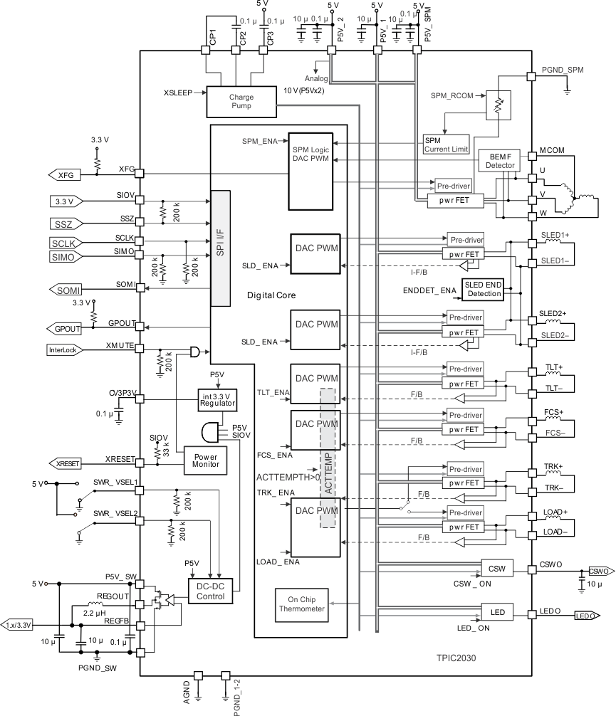
TPIC2030 is low noise type motor driver IC suitable for 5V optical disk drives. The 7-channel driver IC controlled by serial I/F is optimum for driving a spindle motor, a sled motor (stepping motor applicable), a load motor, and Focus / Tracking / Tilt actuators. The integrated current sense resistance for spindle motor current measurement reduces drive system cost. The spindle motor driver part uses integrated sensorless logic to attain very low-noise operation during startup and runtime. By using BEMF feedback, external sensors, such as a Hall device, are not needed to carry out self-starting by the starting circuit or perform position detection. By using the efficient PWM drivers, low-power operation can be achieved by controlling the PWM outputs. Dead zone less control is possible for a Focus / Tracking / Tilt actuator driver. In addition, the spindle part output current limiting circuit, the thermal shut down circuit, and the sled end-detection circuit offer protection for all actuators and motors.
8.2 Functional Block Diagram
8.3 Feature Description
8.3.1 Protection Functions
TPIC2030 has five protection features, under voltage lock out (UVLO), over voltage protection (OVP), short circuit protection (SCP), thermal protection (TSD), and actuator temperature protection (ACTTIMER) in order to protect target equipment. A protect behavior differ by generated events.
8.3.1.1 Undervoltage Lockout (UVLO)
Power faults are reported in the UVLOMon register. Each UVLOMon bit will be initialized to zero upon a cold power up.
After a fault is detected the appropriate fault bit will be latched high. Writing to the RST_ERRFLG (REG77) will clear all UVLOMon bits. The power device faults and actions are summarized in Table 1.
Table 1. Power Fault Monitor
| FAULT TYPE | LATCHED REGISTER | XRESET | CRITERIA | SPM | ACTUATOR | DC-DC |
|---|---|---|---|---|---|---|
| P5V under voltage | UVLO_P5V | Yes | <3.7 V | Hi-Z | Hi-Z | REGOUT = Hi-Z REGFB = GND (enable DC-DC) |
| Internal 3.3 V under voltage | UVLO_INT3P3 | Yes | <2.6 V | Hi-Z | Hi-Z | Hi-Z |
| DC-DC output under voltage | UVLO_SWR | Yes | <80% | Hi-Z | Hi-Z | |
| SIOV under voltage | UVLO_SIOV | Yes | <2.5 V | Hi-Z | Hi-Z | |
| P5V over voltage | OVP_P5V | >6.2 V | Brake | – | – | |
| >6.5 V | Hi-Z | Hi-Z | Hi-Z |
8.3.1.2 Overvoltage Protection (OVP)
Over voltage protect function is aimed to protect the unit from the supplying hi-voltage.
When the supply voltage exceeds 6.5 V, all driver and DC-DC converter output goes Hi-Z. When the supply voltage falls below typical 6.2 V, (6.0 V for SPM) all output start to operate again. The OVP and POR (XRESET) function is not interlocking. However, DC-DC converter output falls by Hi-Z operations, output voltage falls to 80% then XRESET signal goes low.
Moreover, when power supply exceeds 6.2 V, especially SPM enter short brake mode. This operation is offered supposing a voltage rising by motor BEMF of the high velocity revolution.
This function is for insurance, so it can not assure that the device is safety in the condition. Because the absolute maximum ratings range of the supply voltage is 6 V. When this function works, the feed back terminals are not shorted to GND.
Figure 5 shows the behavior of over voltage protection.
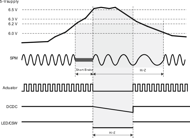 Figure 5. Overvoltage Protection
8.3.1.3 Overcurrent Protection (OCP)
The over current protect function serve to protect the device from break down by large current. The OCP is provided for four circuit blocks, and each threshold are on Table 2.
Table 2. OCP Threshold
| BLOCK | DETECTION CURRENT | MONITOR TIME | PROTECTION TIME | LATCHED FLAG |
|---|---|---|---|---|
| DC-DC converter | 1850 mA (1.x V) 1200 mA (3.3 V) |
1 ms | Forever (P5V power recycle) |
OCP_SWR |
| Load driver 1 channel | Continue 100% duty | 800 ms | forever | OCP_LOAD |
| Load driver 0.5 channel | 240 mA | 800 ms | forever | OCP_LOAD |
| LED driver | 100 mA | 20 µs | 0.4 ms | OCP_LED |
| CSW driver | 500 mA | 20 µs | 1.6 ms | OCP_CSW |
When the large current is detected on each block, device put the output FET to Hi-Z.
The amounts of currents and time have specified the detection threshold for every circuit block.
When OCP occurs, it returns automatically after expiring set Hi-Z period. However, it restricts, the POR is performed at OCP for DC-DC converter. It keeps XRESET = L and does not return forever. It’s necessary power ON/OFF actuation in order to make it release.
OCPERR (REG7F) and OCP flag (REG7B) are set at OCP detection.
8.3.1.3.1 OCP for DC-DC Converter
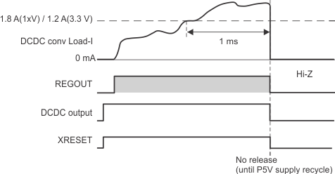 Figure 6. Overcurrent Protection DC-DC Converter
8.3.1.3.2 OCP for Load Driver
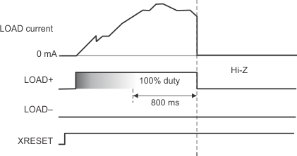 Figure 7. Overcurrent Protection Load 1-Channel
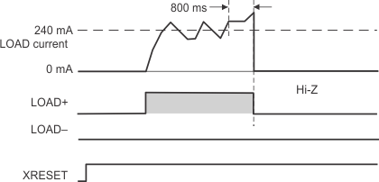 Figure 8. Overcurrent Protection Load 0.5-Channel
8.3.1.3.3 OCP for LED Driver
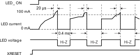 Figure 9. Overcurrent Protection LED Driver
8.3.1.3.4 OCP for CSW
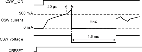 Figure 10. Overcurrent Protection Current Switch
8.3.1.3.4.1 Short Circuit Protection (SCP)
SCP function always monitors the output voltage of high-side and low-side FET of output driver, and when the setting voltage is not outputted, it recognizes as SCP and changed output Hi-Z. It returns to the original state automatically 1.6 ms after.
Table 3. SCP Condition
| BLOCK | FUNCTION | DETECTION CONDITION | DETECT TIME | HI-Z HOLD TIME |
|---|---|---|---|---|
| SPM driver | SCP | Monitor driver output voltage High-side FET output V = GND Low-side FET output V = Supply V |
0.8 to 1.6 µs | 1.6 ms |
| Sled driver | ||||
| Load driver | ||||
| Actuator driver |
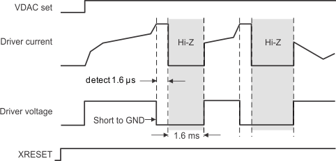 Figure 11. Example of SCP (Driver Short to GND)
8.3.1.4 Thermal Protection (TSD)
The thermal protection (TSD) is a protect function which intercepts an output and suspends an operation when the IC temperature exceed a maximum permissible on a safety. TSD makes an output Hi-Z when the temperature rises up and a threshold value is exceeded. There are two levels for threshold Alert and Trip. Alarm is given by status register TSD_FAULT_ on Alert level with 135°C. It continues rising up temperature, the register TSD_ is set at 150°C and the driver output changes HI-Z. If temperature falls and is reached 135 degrees, it will output again.
TPIC2030 has total 11 temperature sensors in each circuit block. Particular sensor is assigned to appropriate status flag in Table 4.
Table 4. Thermal Sensor Assignment
| CIRCUIT | ALERT (°C) | TRIP (°C) | RELEASE (°C) | ALERT FLAG | TRIP FLAG |
|---|---|---|---|---|---|
| U | 135 | 150 | 135 | TSD_FAULT_SPM | TSD_SPM |
| V | 135 | 150 | 135 | TSD_FAULT_SPM | TSD_SPM |
| W | 135 | 150 | 135 | TSD_FAULT_SPM | TSD_SPM |
| TLT | 135 | 150 | 135 | TSD_FAULT_ACT | TSD_ACT |
| FCS | 135 | 150 | 135 | TSD_FAULT_ACT | TSD_ACT |
| TRK | 135 | 150 | 135 | TSD_FAULT_ACT | TSD_ACT |
| SLED1 | 135 | 150 | 135 | TSD_FAULT_ACT | TSD_ACT |
| SLED2 | 135 | 150 | 135 | TSD_FAULT_ACT | TSD_ACT |
| LOAD | 135 | 150 | 135 | TSD_FAULT_ACT | TSD_ACT |
| LED/CSW | 135 | 150 | 135 | TSD_FAULT_LEDCSW | TSD_ LEDCSW |
| DCDC | 135 | 150 | 135 | TSD_FAULT_SWR | TSD_SWR |
8.3.1.5 Actuator Temperature Protection (ACTTIMER)
TPIC2030 has an actuator protect function named ACTTIMER. This function protects the IC by setting actuator channel output to HIZ when actuator coil current exceeds the specific value. This circuitry calculates heat accumulation to protect the actuators. When this function operates, sled1, 2 and load channel output will be Hi-Z, too. And spindle channel will be forced Auto short brake and disc motor will stop.
It’s able to know the protection has occurred by checking Fault register ACTTIMER_FAULT (REG7F) and ACT_TIMER_PROT (REG78). ACTTIMER_FAULT has a character of advance notice, is set before detecting ACT_TIMER_PROT. Once an ACT_TIMER_PROT is set, even if temperature falls, it will not release protection automatically. It is necessary to clear the flag by setting RST_ERR_FLAG (REG77) or setting 0 to ACTTEMPTH (REG72). ACTTIMER function is able to disable by setting H to ACTPROT_OFF (REG72) or setting 0 to ACTTEMPTH (REG72).
In order to acquire the optimal value for ACTTEMPTH, you should set device into the condition of the detection level, and reading the value of ACTTEMP. Because of the present value can be read from ACTTEMP (REG78). (1)
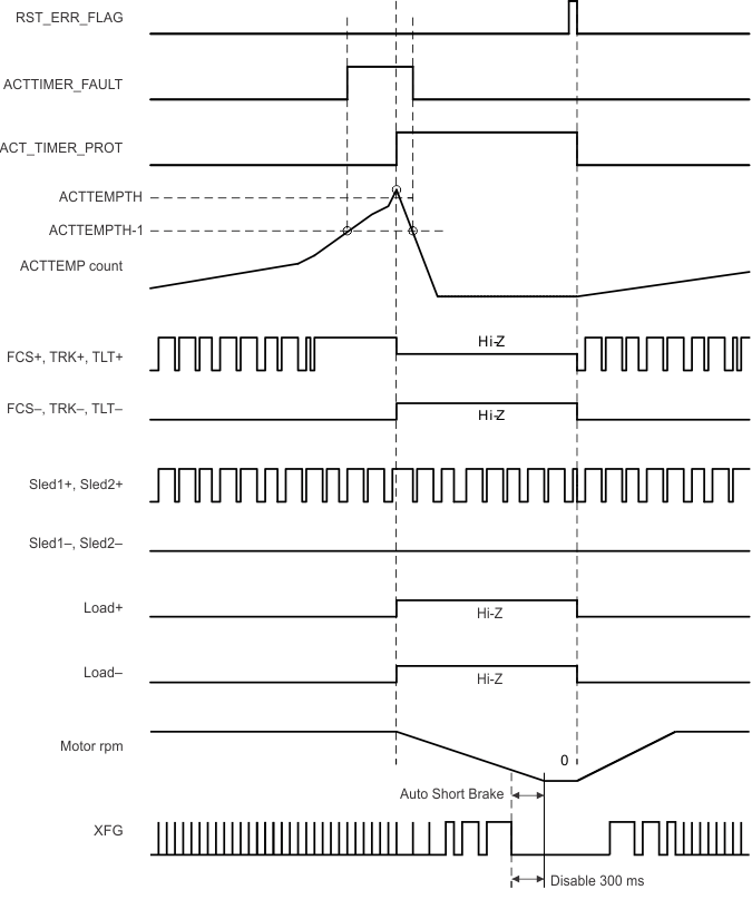 Figure 12. Actuator Temperature Protections
8.4 Device Functional Modes
8.4.1 Power-On Reset (POR)
8.4.1.1 Power-Up Sequences
In TPIC2030, the normal sequence is to wait for 5-V supply to come up to 2.2 V. After 5 V establish, the internal 3.3 V will start and wait until stabilize. Now the voltage monitors start to work and begin to look for the DC-DC converter output. DC-DC converters stabilize the power up sequence finishes and the part starts to function. Once the part finishes all of its power up tasks, it takes XRESET high to indicate that the part is no longer in reset and ready to communicate to the outside world. All the DC-DC converter have soft-start features to avoid rush current and voltage over shoot. Each soft-start sequence takes about 0.8 ms.
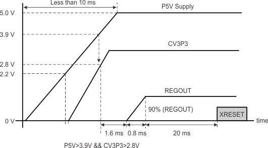 Figure 13. POR (Enable DCDC)
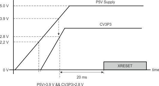 Figure 14. POR (Disable DCDC)
8.4.1.2 XRESET
TPIC2030 is preparing XRESET pin in order to notify an own status to DSP. TPIC2030 set XRESET to L when the event which has a serious effect on DSP occurs such like the power failure, the over temperature and the drop of DCDC converter output. If all the exception is removed, it will tell that XRESET pin would be set to H and it would be in the ready state. The POR (power-on reset) condition is shown in Figure 15. All the behavior of XRESET is shown in Figure 16.
 Figure 15. POR Block Diagram
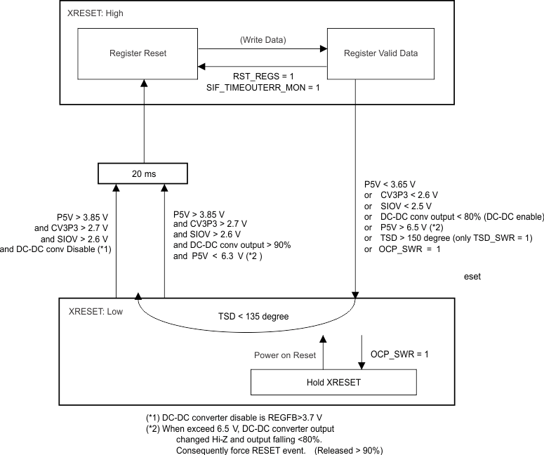 Figure 16. XRESET Behavior
8.4.2 XMUTE
If XMUTE signal is inputted during operation, all the outputs will be suspended and the danger will be avoided.
TPIC2030 will turn off all enable bits, actuator (TLT_ENA/FCS_ENA/TRK_ENA), SPM_ENA, SLD_ENA, LOAD_ENA and CSW_ON when XMUTE input change to L. LOAD_ENA bit will be disabled only when LOAD_05CH =1. Also log this event to error latch flag XMUTE_DETECT (REG79) and PWRERR (REG7F).
If XMUTE_NORST (REG7F) = 1, change of XMUTE will not influence to enable bits.
8.5 Programming
8.5.1 Serial Port Functional Description
The serial communication of TPIC2030 is based on a SPI communications protocol. TPIC2030 is put on the slave side.
All 16-bit transmission data is effective in SSZ=L period.
The bit stream sent through SIMO from a master (DSP) is latched to an internal shift register by the rising edge of SCLK. All the data is transmitted in a total of 16-bit format of a command and data. A format has two types of data, 8 bits and 12 bits length. In order to access specific registers, an address and R/W flag are specified as a command part. In addition, 12 bit data do not have R/W flag in the packet because DAC register ( =12bit data form) are Write only. A transfer packet, command and data, is transmitted sequentially from MSB to LSB. A packet is distinguished in MSB 2 bits of command. In the case of 11, it handles a packet for control register access, and the other processed as a packet for a DAC data setting.
There are the following four kinds of serial-data communication packets.
- Write 12 bits DAC data (MSB two bit ≠ 11)
- Write 8 bits control register (MSB two bit = 11)
- Read 8 bits control register (MSB two bit = 11)
- Write 12 bits Focus DAC data+Read 8 bits status register at the same time (MSB two bit ≠ 11)
8.5.2 Write Operation
For write operation, DSP transmits 16 bit (command + address + data) data a bit every in an order from MSB.
Only the 16-bit data which means 16 SCLK sent from the master during SSZ=L becomes effective. If more than 17 or less than 15 SCLK pulses are received during the time that SSZ is low, the whole packet will be ignored. For all valid write operations, the data of the shift register is latched into its designated internal register at rising edge of 16th SCLK. All internal register bits, except indicated otherwise, are reset to their default states upon power-on-reset.
 Figure 17. Write 12-Bits DAC Data
 Figure 18. Write 8-Bits Control Register
8.5.3 Read Operation
DSP sends 8-bit header through SIMO, in order to perform Read operation. TPIC2030 will start to drive the SOMI line upon the eighth falling edge of SCLK and shift out eight data bits. The master DSP inputs 8-bits data from SOMI after the ninth rising edge of SCLK. There is optional read mode that SOMI data is advanced a half clock cycle of SCLK. This mode becomes effective by setting ADVANCE_RD (REG74) = H.
 Figure 19. Read 8-Bits Control Register
8.5.4 Write and Read Operation
Optionally, the master DSP can read Status register during writing 12 bits DAC (Focus DAC) packet. It’s enabled by setting bit RDSTAT_ON_VFCS (REG74) = H.
 Figure 20. Write 12-Bits Focus DAC Data + Read 8-Bits Status Data
8.6 Register Maps
All registers are in WRITE-protect mode after XRESET release. WRITE_ENA bit (REG76) = H is required before writing data in register.
8.6.1 Register State Transition
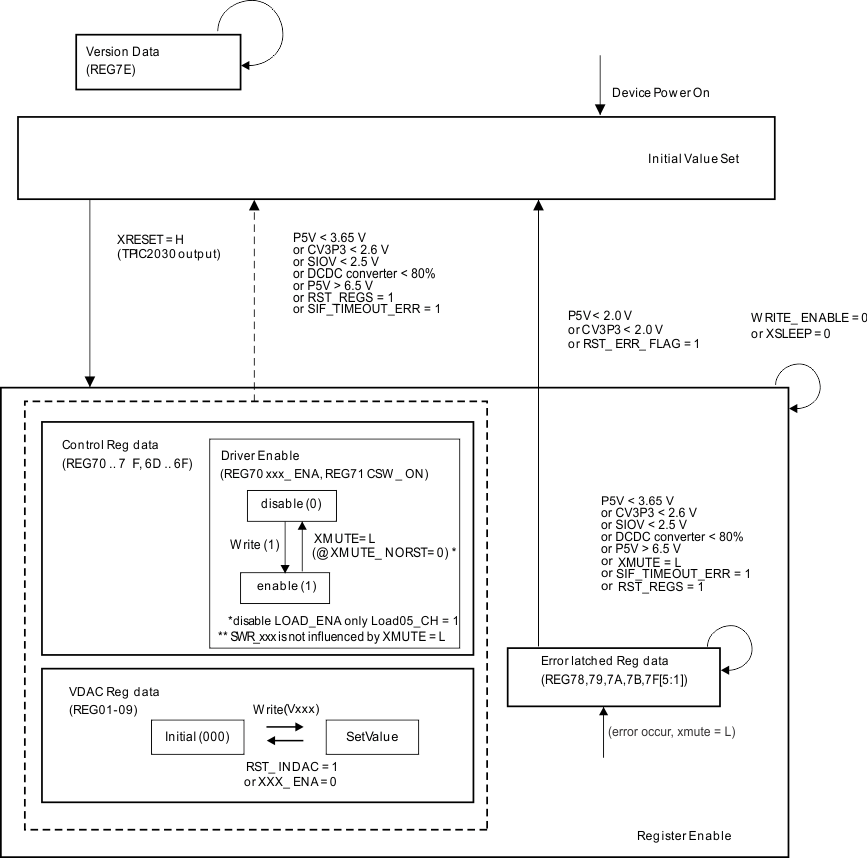 Figure 21. Register State Transition Chart
8.6.2 DAC Register (12-Bit Write Only)
Two difference forms are prepared in 12-bit DAC register, and the forms can be selected by setting VDAC_MAPSW (REG74h).
Table 5. DAC Register (VDAC_MAPSW = 0)
| REG | NAME | F | 11 | 10 | 9 | 8 | 7 | 6 | 5 | 4 | 3 | 2 | 1 | 0 |
|---|---|---|---|---|---|---|---|---|---|---|---|---|---|---|
| 00h | N/A | W | N/A | N/A | N/A | |||||||||
| 01h | VTLT | W | VTLT[11] | VTLT[10] | VTLT[9] | VTLT[8] | VTLT[7] | VTLT[6] | VTLT[5] | VTLT[4] | VTLT[3] | VTLT[2] | VTLT[1] | VTLT[0] |
| 02h | VFCS | W | VFCS[11] | VFCS[10] | VFCS[9] | VFCS[8] | VFCS[7] | VFCS[6] | VFCS[5] | VFCS[4] | VFCS[3] | VFCS[2] | VFCS[1] | VFCS[0] |
| 03h | VTRK | W | VTRK[11] | VTRK[10] | VTRK[9] | VTRK[8] | VTRK[7] | VTRK[6] | VTRK[5] | VTRK[4] | VTRK[3] | VTRK[2] | VTRK[1] | VTRK[0] |
| 04h | VSLD1 | W | VSLD1[11] | VSLD1[10] | VSLD1[9] | VSLD1[8] | VSLD1[7] | VSLD1[6] | VSLD1[5] | VSLD1[4] | VSLD1[3] | VSLD1[2] | VSLD1[1](1) | VSLD1[0] (1) |
| 05h | VSLD2 | W | VSLD2[11] | VSLD2[10] | VSLD2[9] | VSLD2[8] | VSLD2[7] | VSLD2[6] | VSLD2[5] | VSLD2[4] | VSLD2[3] | VSLD2[2] | VSLD2[1] (1) | VSLD2[0] (1) |
| 06h | N/A | W | N/A | N/A | N/A | |||||||||
| 07h | N/A | W | N/A | N/A | N/A | |||||||||
| 08h | VSPM | W | VSPM[11] | VSPM[10] | VSPM[9] | VSPM[8] | VSPM[7] | VSPM[6] | VSPM[5] | VSPM[4] | VSPM[3] | VSPM[2] | VSPM[1] | VSPM[0] |
| 09h | VLOAD | W | VLOAD[11] | VLOAD[10] | VLOAD[9] | VLOAD[8] | VLOAD[7] | VLOAD[6] | VLOAD[5] | VLOAD[4] | VLOAD[3] | VLOAD[2] | VLOAD[1] | VLOAD[0] |
| 0Ah | N/A | W | N/A | N/A | N/A | |||||||||
| 0Bh | N/A | W | N/A | N/A | N/A | |||||||||
Table 6. DAC Register (VDAC_MAPSW = 1)
| REG | NAME | F | 11 | 10 | 9 | 8 | 7 | 6 | 5 | 4 | 3 | 2 | 1 | 0 |
|---|---|---|---|---|---|---|---|---|---|---|---|---|---|---|
| 00h | N/A | W | N/A | N/A | N/A | |||||||||
| 01h | VTLT | W | VTRK[11] | VTRK[10] | VTRK[9] | VTRK[8] | VTRK[7] | VTRK[6] | VTRK[5] | VTRK[4] | VTRK[3] | VTRK[2] | VTRK[1] | VTRK[0] |
| 02h | VFCS | W | VFCS[11] | VFCS[10] | VFCS[9] | VFCS[8] | VFCS[7] | VFCS[6] | VFCS[5] | VFCS[4] | VFCS[3] | VFCS[2] | VFCS[1] | VFCS[0] |
| 03h | VTRK | W | VTLT[11] | VTLT[10] | VTLT[9] | VTLT[8] | VTLT[7] | VTLT[6] | VTLT[5] | VTLT[4] | VTLT[3] | VTLT[2] | VTLT[1] | VTLT[0] |
| 04h | VSLD1 | W | VSLD1[11] | VSLD1[10] | VSLD1[9] | VSLD1[8] | VSLD1[7] | VSLD1[6] | VSLD1[5] | VSLD1[4] | VSLD1[3] | VSLD1[2] | VSLD1[1] (1) | VSLD1[0] (1) |
| 05h | VSLD2 | W | VSLD2[11] | VSLD2[10] | VSLD2[9] | VSLD2[8] | VSLD2[7] | VSLD2[6] | VSLD2[5] | VSLD2[4] | VSLD2[3] | VSLD2[2] | VSLD2[1] (1) | VSLD2[0] (1) |
| 06h | VSPM | W | VSPM[11] | VSPM[10] | VSPM[9] | VSPM[8] | VSPM[7] | VSPM[6] | VSPM[5] | VSPM[4] | VSPM[3] | VSPM[2] | VSPM[1] | VSPM[0] |
| 07h | N/A | W | N/A | N/A | N/A | |||||||||
| 08h | N/A | W | N/A | N/A | N/A | |||||||||
| 09h | VLOAD | W | N/A | VLOAD[11] | VLOAD[10] | VLOAD[9] | VLOAD[8] | VLOAD[7] | VLOAD[6] | VLOAD[5] | VLOAD[4] | |||
| 0Ah | N/A | W | N/A | N/A | N/A | |||||||||
| 0Bh | N/A | W | N/A | N/A | N/A | |||||||||
8.6.3 Control Register
Table 7. Control Register (8bit Read/Write) (1)
| REG | NAME | F | 7 | 6 | 5 | 4 | 3 | 2 | 1 | 0 |
|---|---|---|---|---|---|---|---|---|---|---|
| 70h | DriverEna | R/W | TLT_ENA | FCS_ENA | TRK_ENA | SPM_ENA | SLD_ENA | SWR_MD_BURST | LOAD_ENA | XSLEEP |
| 71h | FuncEna | R/W | SPM_LSMODE | ENDDET_ENA | SWR_BSTAUTON | LED_ON | CSW_ON | TEMPMON_ENA | TI reserved | |
| 72h | ACTCfg | R/W | LOAD_O5CH_HIGH | LOADPROT_OFF | ACTPROT_OFF | ACTTEMPTH | ||||
| 73h | Parm0 | R/W | SIF_TIMEOUT_TH | SLEDEND_HZTIME | SLDENDTH | SPM_RCOM_SEL | XMUTE_NORST | |||
| 74h | OptSet | R/W | DIFF_TLT | LOAD05_CH | STATUS_ON_VFCS | VSLD2_POL | LOAD_OCP_IUP | TI reserved | SOMI_HIZ | VDAC_MAPSW |
| 75h | Protect | R/W | TI reserved | |||||||
| 76h | WriteEna | R/W | WRITE_ENABLE | TI reserved | ||||||
| 77h | ClrReg | W | RST_INDAC | RST_REGS | RST_ERR_FLAG | TI reserved | ||||
| 78h | ActTemp | R | TI reserved | ACT_TIMER_PROT | ACTTEMP | |||||
| 79h | UVLOMon | R | TI reserved | XMUTE_DETECT | UVLO_P5V | UVLO_INT3P3 | UVLO_SIOV | UVLO_SWR | OVP_P5V | |
| 7Ah | TsdMon | R | TSD_FAULT_SWR | TSD_FAULT_SPM | TSD_FAULT_ACT | TSD_FAULT_LEDCSW | TSD_SWR | TSD_SPM | TSD_ACT | TSD_ LEDCSW |
| 7Bh | ProtMon | R | OCP_SWR | OCP_LOAD | OCP_LED | OCP_CSW | SCP_SPM | SCP_SLED | SCP_LOAD | SCP_ACT |
| 7Ch | TempMon | R | CHIPTEMP_STATUS | CHIPTEMP | ||||||
| 7Dh | Protect | R | TI reserved | |||||||
| 7Eh | Version | R | Version | |||||||
| 7Fh | Status | R | ACTTIMER_FAULT | ENDDET | SIF_TIMEOUTERR | PWRERR | TSDERR | OCPSCPERR | TSDFAULT | FG |
| 60h | Protect | R/W | TI reserved | |||||||
| 61h | Protect | R/W | TI reserved | |||||||
| 62h | Protect | R/W | TI reserved | |||||||
| 63h | Protect | R/W | TI reserved | |||||||
| 64h | Protect | R/W | TI reserved | |||||||
| 65h | Protect | R/W | TI reserved | FBSVR_SBRK_OFF | TI reserved | |||||
| 66h | Protect | R/W | TI reserved | |||||||
| 6Ah | Protect | R/W | TI reserved | |||||||
| 6Ch | Protect | R/W | TI reserved | |||||||
| 6Dh | DCCfg | R/W | TI reserved | SWR_BST_HEFF | TI reserved | SWR_VOUTUP | ||||
| 6Eh | UtilCfg | R/W | GPOUT_HL | GPOUT_ENA | TI reserved | SWR_GPIO_CNTL | TI reserved | |||
| 6Fh | MonitorSet | R/W | ACTTIMER_FLT_MON | ENDDET_MON | SIF_TIMEOUTERR_MON | PWRERR_MON | TSDERR_MON | OCPSCPERR_MON | TSDFAULT_MON | TI reserved |
8.6.4 Detailed Description of Registers
8.6.4.1 REG01 12-bit DAC for Tilt (VDAC_MAPSW = 0)
| 15 | 14 | 13 | 12 | 11 | 10 | 9 | 8 |
| VTLT | |||||||
| w-0 | w-0 | w-0 | w-0 | ||||
| 7 | 6 | 5 | 4 | 3 | 2 | 1 | 0 |
| VTLT | |||||||
| w-0 | w-0 | w-0 | w-0 | w-0 | w-0 | w-0 | w-0 |
| LEGEND: R/W = Read/Write; R = Read only; -n = value after reset |
Table 8. Tilt (REG01) Field Descriptions
| Bit | Field | Type | Default | Description |
|---|---|---|---|---|
| 11-0 | VTLT | w | 0 | Digital input code for Tilt. 2’s compliment format 0x800(-2048) to 0x7ff(+2047) Output is changed by differential Tilt mode (REG74[7]) TLT_OUT = VTLT* (6.0/2048) (DIFF_TLT=0) TLT_OUT = (VFCS-VTLT)* (6.0/2048) (DIFF_TLT=1)TLT_OUT should be changed after writing VFCS. In DIFF_TLT mode (DIFF_TLT=1), TLT_OUT should be changed after writing VFCS. |
8.6.4.2 REG02 12-bit DAC for Focus (VDAC_MAPSW = 0)
| 15 | 14 | 13 | 12 | 11 | 10 | 9 | 8 |
| VFCS | |||||||
| w-0 | w-0 | w-0 | w-0 | ||||
| 7 | 6 | 5 | 4 | 3 | 2 | 1 | 0 |
| VFCS | |||||||
| w-0 | w-0 | w-0 | w-0 | w-0 | w-0 | w-0 | w-0 |
| LEGEND: R/W = Read/Write; R = Read only; -n = value after reset |
Table 9. Focus (REG02) Field Descriptions
| Bit | Field | Type | Default | Description |
|---|---|---|---|---|
| 11-0 | VFCS | w | 0 | Digital input code for Focus. 2’s compliment format 0x800(-2048) to 0x7ff(+2047) Output is changed by differential Tilt mode (REG74[7]) FCS_OUT = VFCS × (6.0/2048) (DIFF_TLT=0) FCS_OUT = (VFCS+VTLT)* (6.0/2048) (DIFF_TLT=1) |
8.6.4.3 REG03 12-bit DAC for Track (VDAC_MAPSW = 0)
| 15 | 14 | 13 | 12 | 11 | 10 | 9 | 8 |
| VTRK | |||||||
| w-0 | w-0 | w-0 | w-0 | ||||
| 7 | 6 | 5 | 4 | 3 | 2 | 1 | 0 |
| VTRK | |||||||
| w-0 | w-0 | w-0 | w-0 | w-0 | w-0 | w-0 | w-0 |
| LEGEND: R/W = Read/Write; R = Read only; -n = value after reset |
Table 10. Track (REG03) Field Descriptions
| Bit | Field | Type | Default | Description |
|---|---|---|---|---|
| 11-0 | VTRK | w | 0 | Digital input code for Tracking. 2’s compliment format 0x800(-2048) to 0x7ff(+2047) TRK_OUT = VTRK* (6.0/2048) |
8.6.4.4 REG04 10bit DAC for Sled1 (VDAC_MAPSW = 0)
| 15 | 14 | 13 | 12 | 11 | 10 | 9 | 8 |
| VSLD1 | |||||||
| w-0 | w-0 | w-0 | w-0 | ||||
| 7 | 6 | 5 | 4 | 3 | 2 | 1 | 0 |
| VSLD1 | |||||||
| w-0 | w-0 | w-0 | w-0 | w-0 | w-0 | w-0 | w-0 |
| LEGEND: R/W = Read/Write; R = Read only; -n = value after reset |
Table 11. Sled1 (REG04) Field Descriptions
| Bit | Field | Type | Default | Description |
|---|---|---|---|---|
| 11-2 | VSLD1 | w | 0 | Digital input code for Sled1. 2’s compliment format 0x800(-2048) to 0x7ff(+2047) Two bits on LSB, VSLD1[1:0], will be handled with zero. SLD1_OUT = VSLD1* (440mA/2048) |
| 1-0 | TI reserved |
8.6.4.5 REG05 10bit DAC for Sled2 (VDAC_MAPSW = 0)
| 15 | 14 | 13 | 12 | 11 | 10 | 9 | 8 |
| VSLD2 | |||||||
| w-0 | w-0 | w-0 | w-0 | ||||
| 7 | 6 | 5 | 4 | 3 | 2 | 1 | 0 |
| VSLD2 | |||||||
| w-0 | w-0 | w-0 | w-0 | w-0 | w-0 | w-0 | w-0 |
| LEGEND: R/W = Read/Write; R = Read only; -n = value after reset |
Table 12. Sled2 (REG05) Field Descriptions
| Bit | Field | Type | Default | Description |
|---|---|---|---|---|
| 11-2 | VSLD2 | w | 0 | Digital input code for Sled2. 2’s compliment format 0x800(-2048) to 0x7ff(+2047) Two bits on LSB, VSLD2[1:0], will be handled with zero. SLD2_OUT = VSLD2* (440mA/2048) |
| 1-0 | TI reserved |
8.6.4.6 REG08 12-bit DAC for Spindle (VDAC_MAPSW = 0)
| 15 | 14 | 13 | 12 | 11 | 10 | 9 | 8 |
| VSPM | |||||||
| w-0 | w-0 | w-0 | w-0 | ||||
| 7 | 6 | 5 | 4 | 3 | 2 | 1 | 0 |
| VSPM | |||||||
| w-0 | w-0 | w-0 | w-0 | w-0 | w-0 | w-0 | w-0 |
| LEGEND: R/W = Read/Write; R = Read only; -n = value after reset |
Table 13. Spindle (REG08) Field Descriptions
| Bit | Field | Type | Default | Description |
|---|---|---|---|---|
| 11-0 | VSPM | w | 0 | Digital input code for Spindle. 2’s compliment format 0x800(-2048) to 0x7ff(+2047) SPM_OUT = VSPM* (6.0/2048) |
8.6.4.7 REG09 12-bit DAC for Load (VDAC_MAPSW = 0)
| 15 | 14 | 13 | 12 | 11 | 10 | 9 | 8 |
| VLOAD | |||||||
| w-0 | w-0 | w-0 | w-0 | ||||
| 7 | 6 | 5 | 4 | 3 | 2 | 1 | 0 |
| VLOAD | |||||||
| w-0 | w-0 | w-0 | w-0 | w-0 | w-0 | w-0 | w-0 |
| LEGEND: R/W = Read/Write; R = Read only; -n = value after reset |
Table 14. Load (REG09) Field Descriptions
| Bit | Field | Type | Default | Description |
|---|---|---|---|---|
| 11-0 | VLOAD | w | 0 | Digital input code for Load. 2’s compliment format 0x800(-2048) to 0x7ff(+2047) LOAD_OUT = VLOAD* (6.0/2048) |
8.6.4.8 REG65 8bit Control Register for FBSVR
| 7 | 6 | 5 | 4 | 3 | 2 | 1 | 0 |
| TI reserved | FBSVR_SBRK_OFF | TI reserved | |||||
| rw-0 | rw-0 | rw-0 | rw-0 | rw-0 | rw-0 | rw-0 | rw-0 |
| LEGEND: R/W = Read/Write; R = Read only; -n = value after reset |
Table 15. FBSVR (REG65) Field Descriptions(1)
| Bit | Field | Type | Default | Description |
|---|---|---|---|---|
| 7-2 | TI reserved | rw | 0 | |
| 1 | FBSVR_SBRK_OFF | rw | 0 | SPM FB saver mode 0: Reset only when F/R transition (Default) 1: Reset all time when SBRK (Recommend) |
| 0 | TI reserved | rw | 0 |
8.6.4.9 REG6D 8bit Control Register for DCCfg
| 7 | 6 | 5 | 4 | 3 | 2 | 1 | 0 |
| TI reserved | SWR_BST_HEFF | TI reserved | SWR_VOUTUP | ||||
| rw-0 | rw-0 | rw-0 | rw-0 | rw-0 | rw-0 | rw-0 | rw-0 |
| LEGEND: R/W = Read/Write; R = Read only; -n = value after reset |
Table 16. DCCfg (REG6D) Field Descriptions
| Bit | Field | Type | Default | Description |
|---|---|---|---|---|
| 7-6 | TI reserved | rw | 0 | |
| 5 | SWR_BST_HEFF | rw | 0 | Select high efficiency mode in discontinuous mode (for 1.xV only) 0: normal regulation 1: high efficiency mode |
| 4-2 | TI reserved | rw | 0 | |
| 1-0 | SWR_VOUTUP | rw | 0 | DCDC converter output voltage up. (for 1.xV only) 00: 0%, 01: 2% 10: 3.8% 11: 5.4% (for 1.2V, 1.5V) 00: 0%, 01: 1.3% 10: 2.4% 11: 3.3% (for 1.0V) Prohibit setting in 3.3V output mode. |
8.6.4.10 REG6E 8bit Control Register for UtilCfg
| 7 | 6 | 5 | 4 | 3 | 2 | 1 | 0 |
| GPOUT_HL | GPOUT_ENA | TI reserved | SWR_GPIO_CNTL | TI reserved | |||
| rw-0 | rw-0 | rw-0 | rw-0 | rw-0 | rw-0 | rw-0 | rw-0 |
| LEGEND: R/W = Read/Write; R = Read only; -n = value after reset |
Table 17. UtilCfg (REG6E) Field Descriptions
| Bit | Field | Type | Default | Description |
|---|---|---|---|---|
| 7 | GPOUT_HL | rw | 0 | GPOUT (General Purpose Output) pin output selection 0: low output 1: high output valid only REG6F=00h |
| 6 | GPOUT_ENA | rw | 0 | Enable monitor signal output to GPOUT pin 0: No signal output, Hi-Z 1: output signal selected in REG6F with CMOS output Output is Logical OR when selected two more signals |
| 4 | SWR_GPIO_CNTL | rw | 0 | Set GPOUT output value (disable DCDC converter) 0: output L in REGOUT pin (open drain) 1: output H in REGOUT pin (open drain) |
| 3-0 | TI reserved | rw | 0 |
8.6.4.11 REG6F 8bit Control Register for MonitorSet (REG6F)
| 7 | 6 | 5 | 4 | 3 | 2 | 1 | 0 |
| ACTTIMER_FLT_MON | ENDDET_MON | SIF_TIMEOUTERR_MON | PWRERR_MON | TSDERR_MON | OCPERR_MON | TSDFAULT_MON | TI reserved |
| rw-0 | rw-0 | rw-0 | rw-0 | rw-0 | rw-0 | rw-0 | rw-0 |
| LEGEND: R/W = Read/Write; R = Read only; -n = value after reset |
Table 18. MonitorSet (REG6F) Field Descriptions
| Bit | Field | Type | Default | Description |
|---|---|---|---|---|
| 7 | ACTTIMER_FLT_MON | rw | 0 | Assign signal to GPIO pin 1: ACTTIMER fault output to GPOUT pin |
| 6 | ENDDET_MON | rw | 0 | Assign signal to GPIO pin 1: ENDDET monitor output to GPOUT pin |
| 5 | SIF_TIMEOUTERR_MON | rw | 0 | Assign signal to GPIO pin 1: SIF timeout monitor output to GPOUT pin |
| 4 | PWRERR_MON | rw | 0 | Assign signal to GPIO pin 1: PWRERR monitor output to GPOUT pin |
| 3 | TSDERR_MON | rw | 0 | Assign signal to GPIO pin 1: TSDERR fault output to GPOUT pin |
| 2 | OCPERR_MON | rw | 0 | Assign signal to GPIO pin 1: OCPERR fault output to GPOUT pin |
| 1 | TSDFAULT_MON | rw | 0 | Assign signal to GPIO pin 1: TSDFAULT fault output to GPOUT pin |
| 0 | TI reserved | rw | 0 |
8.6.4.12 REG70 8bit Control Register for DriverEna
| 7 | 6 | 5 | 4 | 3 | 2 | 1 | 0 |
| TLT_ENA | FCS_ENA | TRK_ENA | SPM_ENA | SLD_ENA | SWR_MD_BURST | LOAD_ENA | XSLEEP |
| rw-0 | rw-0 | rw-0 | rw-0 | rw-0 | rw-0 | rw-0 | rw-0 |
| LEGEND: R/W = Read/Write; R = Read only; -n = value after reset |
Table 19. DriverEna (REG70) Field Descriptions
| Bit | Field | Type | Default | Description |
|---|---|---|---|---|
| 7 | TLT_ENA | rw | 0 | 1 : Tilt enable (with XSLEEP=1) It’s reset when XMUTE changes to L. |
| 6 | FCS_ENA | rw | 0 | 1: Focus enable (with XSLEEP=1) It’s reset when XMUTE changes to L. |
| 5 | TRK_ENA | rw | 0 | 1: Track enable (with XSLEEP=1) It’s reset when XMUTE changes to L. |
| 4 | SPM_ENA | rw | 0 | 1: Spindle enable (with XSLEEP=1) It’s reset when XMUTE changes to L. |
| 3 | SLD_ENA | rw | 0 | 1: Sled enable (with XSLEEP=1) It’s reset when XMUTE changes to L. |
| 2 | SWR_MD_BURST | rw | 0 | 1 : Enable DCDC converter discontinuous regulation mode. Regardless of the amount of current consumption, it will always be in discontinuous mode. Holds a former value after XMUTE = L event. |
| 1 | LOAD_ENA | rw | 0 | 1 : LOAD enable (with XSLEEP=1) Track (bit5:TRK_ENA) will be disabled at LOAD_ENA=1 because of sharing the DAC PWM module. Load priority is higher than TRK_ENA. It’s reset when XMUTE changes to L. (with LOAD_05CH=1) |
| 0 | XSLEEP | rw | 0 | 1: Operation mode 0 : Power save mode Charge pump enable bit. All driver enable bit (Bit[7:1]) change disabled and output change to Hi-Z (regardless of setting xxx_ENA bit is 1) when setting XSLEEP to 0. Therefore set 1 to XSLEEP before setting each enable bits. |
8.6.4.13 REG71 8bit Control Register for FuncEna
| 7 | 6 | 5 | 4 | 3 | 2 | 1 | 0 |
| SPM_LSMODE | ENDDET_ENA | SWR_BSTAUTON | LED_ON | CSW_ON | TEMPMON_ENA | TI reserved | |
| rw-0 | rw-0 | rw-0 | rw-0 | rw-0 | rw-0 | rw-0 | rw-0 |
| LEGEND: R/W = Read/Write; R = Read only; -n = value after reset |
Table 20. FuncEna (REG71) Field Descriptions
| Bit | Field | Type | Default | Description |
|---|---|---|---|---|
| 7 | SPM_LSMODE | rw | 0 | 0 : Spindle rotation mode 1 : Light Scribe mode (slow rotation mode) |
| 6 | ENDDET_ENA | rw | 0 | 1 : use Sled end detection enable ( with SLD_ENA=1) |
| 5 | SWR_BSTAUTON | rw | 0 | 1 : Enable auto DCDC converter discontinuous regulation mode. At low current consumption, it changes to discontinuous mode automatically. Holds a former value after XMUTE = L event. SWR_BSTAUTON mode is chosen when both bit SWR_BSTAUTON and SWR_MD_BURST are set. |
| 4 | LED_ON | rw | 0 | 1 : LEDO enable ( with XSLEEP=1) |
| 3 | CSW_ON | rw | 0 | 1 : CSWO enable ( with XSLEEP=1) It’s reset when XMUTE changes to L |
| 2 | TEMPMON_ENA | rw | 0 | 1: enable chip temperature monitoring ( with XSLEEP=1) |
| 1-0 | TI reserved | rw | 0 |
8.6.4.14 REG72 8bit Control Register for ACTCfg
| 7 | 6 | 5 | 4 | 3 | 2 | 1 | 0 |
| LOAD_O5CH_HIGH | LOADPROT_OFF | ACTPROT_OFF | ACTTEMPTH | ||||
| rw-0 | rw-0 | rw-0 | rw-0 | rw-0 | rw-0 | rw-0 | rw-0 |
| LEGEND: R/W = Read/Write; R = Read only; -n = value after reset |
Table 21. ACTCfg (REG72) Field Descriptions
| Bit | Field | Type | Default | Description |
|---|---|---|---|---|
| 7 | LOAD_05CH_HIGH | rw | 0 | LOAD output polarity at 0.5CH ( REG74h[6]=1 ) 0: LOADP=Low 1: LOADP=High |
| 6 | LOADPROT_OFF | rw | 0 | 1: Load Overcurrent Protection OFF |
| 5 | ACTPROT_OFF | rw | 0 | 0 : Actuator protection ON 1 : Actuator Fault monitor disable (No protection for ACT channel) |
| 4-0 | ACTTEMPTH | rw | 0 | Actuator thermal protection (=ACT Timer) threshold level ACT Timer Protection enable except ACTTEMPTH[4:0]=0x00 ACTTEMPTH = 0x00 equal to ACTPROT_OFF = 1 By writing value 0x00, ACTTIMER_PROT flag is cleared. |
8.6.4.15 REG73 8bit Control Register for Parm0
| 7 | 6 | 5 | 4 | 3 | 2 | 1 | 0 |
| SIF_TIMEOUT_TH | SLEDEND_HZTIME | SLDENDTH | SPM_RCOM_SEL | XMUTE_NORST | |||
| rw-0 | rw-0 | rw-0 | rw-0 | rw-0 | rw-0 | rw-0 | rw-0 |
| LEGEND: R/W = Read/Write; R = Read only; -n = value after reset |
Table 22. Parm0 (REG73) Field Descriptions
| Bit | Field | Type | Default | Description |
|---|---|---|---|---|
| 7-6 | SIF_TIMEOUT_TH | rw | 0 | Watch dog timer for Serial communication 0: disable 1: 1 ms 2: 100 µs 3: 10 µs Set SIF_TIMEOUTERR (REG7F) if communication is suspended for this time period. XRESET processing will be performed if a SIF_TIMEOUTERR occurs. |
| 5 | SLEDEND_HZTIME | rw | 0 | Time window for sled end detection. 0: 400 µs 1: 200 µs Caution) Need to recycle ENDDET_ENA=0→1 after writing this bit. |
| 4-3 | SLDENDTH | rw | 0 | Sled end detection sensibility setting. Detection threshold for motor BEMF 00: 46 mV; 01: 86 mV; 10: 0 mV; 11: 22 mV |
| 2-1 | SPM_RCOM_SEL | rw | 0 | Select resistor value of spindle current sense resistor. Current limit is set as following current. 00: 890 mA; 01: 980 mA; 10: 725 mA; 11: 784 mA |
| 0 | XMUTE_NORST | rw | 0 | Reset driver enable bit (XXX_ENA and CSW_ON) register at XMUTE = L. 0: Reset enable bit at XMUTE = L 1: XMUTE status does not influence enable bit. |
8.6.4.16 REG74 8bit Control Register for OptSet
| 7 | 6 | 5 | 4 | 3 | 2 | 1 | 0 |
| DIFF_TLT | LOAD_05CH | RDSTAT_ON_VFCS | VSLD2_POL | LOAD_OCP_ IUP |
TI reserved | SOMI_HIZ | VDAC_MAPSW |
| rw-0 | rw-0 | rw-0 | rw-0 | rw-0 | rw-0 | rw-0 | rw-0 |
| LEGEND: R/W = Read/Write; R = Read only; -n = value after reset |
Table 23. OptSet (REG74) Field Descriptions
| Bit | Field | Type | Default | Description |
|---|---|---|---|---|
| 7 | DIFF_TLT | rw | 0 | 1 : Differential Tilt mode enable (with TLT_ENA=FCS_ENA=1) Differential Tilt mode (DIFF_TLT=1), DAC value setting as follows FCS_OUT = (VFCS + VTLT) × 6 / 2048 TLT_OUT = (VFCS – VTLT) × 6 / 2048 In DIFF_TLT mode (DIFF_TLT = 1), TLT_OUT should be changed after writing VFCS. |
| 6 | LOAD_05CH | rw | 0 | The setting of Load motor driving type. Load output changes as follow 0: step down mode (LOAD output is controlled by DAC code, VLOAD) Use for Slot-in model or step down tray model. 1: 0.5Ch mode (LOAD is only controlled by LOAD_05CH_HIGH) Use for Tray model |
| 5 | RDSTAT_ON_VFCS | rw | 0 | Set Read status data (REG7F) at VFCS write command (REG02) 1: enable Write and Read mode (Write 12-bits Focus DAC data + Read 8bits status data) |
| 4 | VSLD2_POL | rw | 0 | change direction of SLED rotation |
| 3 | LOAD_OCP_IUP | rw | 0 | Select over current protection (OCP) threshold for Load channel current 0: 250mA 1: 425mA |
| 2 | TI reserved | rw | 0 | |
| 1 | SOMI_HIZ | rw | 0 | 0: SOMI line High-Z at bus idling time. 1: SOMI line Pull Down at bus idling time. |
| 0 | VDAC_MAPSW | rw | 0 | Selection of DAC register channel assignments (REG01~09) |
8.6.4.17 REG76 8bit Control Register for WriteEna
| 7 | 6 | 5 | 4 | 3 | 2 | 1 | 0 |
| WRITE_ENABLE | TI reserved | ||||||
| rw-0 | rw-0 | rw-0 | rw-0 | rw-0 | rw-0 | rw-0 | rw-0 |
| LEGEND: R/W = Read/Write; R = Read only; -n = value after reset |
Table 24. WriteEna (REG76) Field Descriptions
| Bit | Field | Type | Default | Description |
|---|---|---|---|---|
| 7 | WRITE_ENABLE | 0 | 0: Register Write disable except REG76 1: Write enable for registers REG01~0B, REG70~7F, REG6C~6F |
|
| 6-0 | TI reserved |
8.6.4.18 REG77 8bit Control Register for ClrReg
| 7 | 6 | 5 | 4 | 3 | 2 | 1 | 0 |
| RST_INDAC | RST_REGS | RST_ERR_FLAG | RST_REGS_WO3 | TI reserved | |||
| w-0 | w-0 | w-0 | w-0 | w-0 | w-0 | w-0 | w-0 |
| LEGEND: R/W = Read/Write; R = Read only; -n = value after reset |
Table 25. ClrReg (REG77) Field Descriptions
| Bit | Field | Type | Default | Description |
|---|---|---|---|---|
| 7 | RST_INDAC | w | 0 | 1 : Reset all 12-bit input DAC register (REG01~0B) *Self clear bit |
| 6 | RST_REGS | w | 0 | 1 : Reset all 8bit R/W Registers (REG70h~77h, 60h-6Fh) *Self clear bit |
| 5 | RST_ERR_FLAG | w | 0 | 1 : Reset Fault Flag Latch (REG7F[5:1], REG79~REG7B) *Self clear bit |
| 4-0 | TI reserved | w | 0 |
8.6.4.19 REG78 8bit Control Register for ActTemp
| 7 | 6 | 5 | 4 | 3 | 2 | 1 | 0 |
| TI reserved | ACT_TIMER_ PROT |
ACTTEMP | |||||
| r-0 | r-0 | r-0 | r-0 | r-0 | r-0 | r-0 | r-0 |
| LEGEND: R/W = Read/Write; R = Read only; -n = value after reset |
Table 26. ActTemp (REG78) Field Descriptions
| Bit | Field | Type | Default | Description |
|---|---|---|---|---|
| 7-6 | TI reserved | r | 0 | |
| 5 | ACT_TIMER_PROT | r | 0 | ACT timer protection flag 1: ACT Timer Protection has detected and latched. (ACTTEMP > ACTTEMPTH) This bit holds data after temperature change to low since this is a latch bit. Also driver output keep Hi-Z until setting RST_ERR_FLAG or ACTTEMPTH=0. |
| 4-0 | ACTTEMP | r | 0 | An integrated value of ACT_TIMER counters at present. |
8.6.4.20 REG79 8bit Control Register for UVLOMon
| 7 | 6 | 5 | 4 | 3 | 2 | 1 | 0 |
| TI reserved | XMUTE_ DETECT |
UVLO_P5V | UVLO_INT3P3 | UVLO_SIOV | UVLO_SWR | OVP_P5V | |
| r-0 | r-0 | r-0 | r-0 | r-0 | r-0 | r-0 | r-0 |
| LEGEND: R/W = Read/Write; R = Read only; -n = value after reset |
Table 27. UVLOMon (REG79) Field Descriptions
| Bit | Field | Type | Default | Description |
|---|---|---|---|---|
| 7-6 | TI reserved | r | 0 | |
| 5 | XMUTE_DETECT | r | 0 | XMUTE flag for detection Lo input. (>20 µs)(1) |
| 4 | UVLO_P5V | r | 0 | UVLO (Under Voltage Lock Out) flag for detection Low P5V supply(1) |
| 3 | UVLO_INT3P3 | r | 0 | UVLO flag for detection Low internal 3.3-V regulator(1) |
| 2 | UVLO_SIOV | r | 0 | UVLO flag for detection Low SIOV(1) |
| 1 | UVLO_SWR | r | 0 | UVLO flag for detection Low DCDC(1) |
| 0 | OVP_P5V | r | 0 | Over voltage protection flag for P5Vsply(1) |
8.6.4.21 REG7A 8bit Control Register for TsdMon
| 7 | 6 | 5 | 4 | 3 | 2 | 1 | 0 |
| TSD_FAULT_SWR | TSD_FAULT_SPM | TSD_FAULT_ACT | TSD_FAULT_LEDCSW | TSD_SWR | TSD_SPM | TSD_ACT | TSD_ LEDCSW |
| r-0 | r-0 | r-0 | r-0 | r-0 | r-0 | r-0 | r-0 |
| LEGEND: R/W = Read/Write; R = Read only; -n = value after reset |
Table 28. TsdMon (REG7A) Field Descriptions
| Bit | Field | Type | Default | Description |
|---|---|---|---|---|
| 7 | TSD_FAULT_SWR | r | 0 | Pre alert of thermal protection for DCDC converter block(1) |
| 6 | TSD_FAULT_SPM | r | 0 | Pre alert of thermal protection of Spindle block(1) |
| 5 | TSD_FAULT_ACT | r | 0 | Pre alert of thermal protection of Focus /Track /Tilt Sled1 /Sled2 / /Load(1) |
| 4 | TSD_FAULT_LEDCSW | r | 0 | Pre alert of thermal protection of CSW/LED(1) |
| 3 | TSD_SWR | r | 0 | Thermal protection flag for DCDC converter block(1)
DCDC converter output Hi-Z until temperature falls on release level 1: detect (latch) |
| 2 | TSD_SPM | r | 0 | Thermal protection flag for Spindle(1)
SPM output Hi-Z until temperature falls on release level 1: detect (latch) |
| 1 | TSD_ACT | r | 0 | Thermal protection flag for Focus /Track /Tilt Sled1 /Sled2 /Load(1)
Actuator output Hi-Z until temperature falls on release level 1: detect (latch) |
| 0 | TSD_ LEDCSW | r | 0 | Thermal protection flag for CSW/LED(1)
LED/CSW output Hi-Z until temperature falls on release level 1: detect (latch) |
8.6.4.22 REG7B 8bit Control Register for ProtMon
| 7 | 6 | 5 | 4 | 3 | 2 | 1 | 0 |
| OCP_SWR | OCP_LOAD | OCP_LED | OCP_CSW | SCP_SPM | SCP_SLED | SCP_LOAD | SCP_ACT |
| r-0 | r-0 | r-0 | r-0 | r-0 | r-0 | r-0 | r-0 |
| LEGEND: R/W = Read/Write; R = Read only; -n = value after reset |
Table 29. ProtMon (REG7B) Field Descriptions
| Bit | Field | Type | Default | Description |
|---|---|---|---|---|
| 7 | OCP_SWR | r | 0 | Overcurrent protection flag bit for DCDC converter(1) |
| 6 | OCP_LOAD | r | 0 | Overcurrent protection flag bit for Load channel(1) |
| 5 | OCP_LED | r | 0 | Overcurrent protection flag bit for LED channel(1) |
| 4 | OCP_CSW | r | 0 | Overcurrent protection flag bit for CSW channel(1) |
| 3 | SCP_SPM | r | 0 | Short circuit protection flag bit for spindle channe(1) |
| 2 | SCP_SLED | r | 0 | Short circuit protection flag bit for sled channe(1) |
| 1 | SCP_LOAD | r | 0 | Short circuit protection flag bit for load channe(1) |
| 0 | SCP_ACT | r | 0 | Short circuit protection flag bit for Fcs/Trk/Tilt channel(1) |
8.6.4.23 REG7C 8bit Control Register for TempMon
| 7 | 6 | 5 | 4 | 3 | 2 | 1 | 0 |
| CHIPTEMP_STATUS | CHIPTEMP | ||||||
| r-0 | r-0 | r-0 | r-0 | r-0 | r-0 | r-0 | r-0 |
| LEGEND: R/W = Read/Write; R = Read only; -n = value after reset |
Table 30. TempMon (REG7C) Field Descriptions
| Bit | Field | Type | Default | Description |
|---|---|---|---|---|
| 7 | CHIPTEMP_STATUS | r | 0 | 1: New data CHIPTEMP[6:0] is updated It will be cleared after reading. |
| 6-0 | CHIPTEMP | r | 0 | Chip temperature monitor (1.2deg/LSB) 15(0) to 165(127) degrees. For monitoring, TEMPMON_ENA=1 and XSLEEP=1 is required |
8.6.4.24 REG7E 8bit Control Register for Version
| 7 | 6 | 5 | 4 | 3 | 2 | 1 | 0 |
| Version | |||||||
| r-0 | r-0 | r-0 | r-0 | r-0 | r-0 | r-0 | r-0 |
| LEGEND: R/W = Read/Write; R = Read only; -n = value after reset |
Table 31. Version (REG7E) Field Descriptions
| Bit | Field | Type | Default | Description |
|---|---|---|---|---|
| 7-0 | Version | r | X | Version[7:4] = revision number of TPIC2030 Version[3:0] = option |
8.6.4.25 REG7F 8bit Control Register for Status
| 7 | 6 | 5 | 4 | 3 | 2 | 1 | 0 |
| ACTTIMER_FAULT | ENDDET | SIF_TIMEOUTERR | PWRERR | TSDERR | OCPERR | TSDFAULT | FG |
| r-0 | r-0 | r-0 | r-0 | r-0 | r-0 | r-0 | r-0 |
| LEGEND: R/W = Read/Write; R = Read only; -n = value after reset |
Table 32. Status (REG7F) Field Descriptions
| Bit | Field | Type | Default | Description |
|---|---|---|---|---|
| 7 | ACTTIMER_FAULT | r | 0 | Status flag of ACTTIMER protection 1: Pre alert of ACTTIMER protection. It is close to the threshold level. You can get current ACTTIMER value in REG78. Both of this bit and ACT_TIMER_PROT (REG78) will be set when over the threshold. |
| 6 | ENDDET | r | 0 | status flag of END detection 1: end position detected (not latch bit) |
| 5 | SIF_TIMEOUTERR | r | 0 | error flag of serial I/F watch dog timer 1: SIF communication was interrupted, expired watch dog timer |
| 4 | PWRERR | r | 0 | error flag of Power 1 : Voltage problem occurred, details in REG79 |
| 3 | TSDERR | r | 0 | error flag of any over thermal protections 1: Dispatched thermal protection, details in REG7A |
| 2 | OCPERR | r | 0 | error flag of any over current protection 1: Dispatched OCP, details in REG7Bh |
| 1 | TSDFAULT | r | 0 | warning of TSD of any thermal protection 1 : Detect pre thermal protection details in REG7A |
| 0 | FG | r | 0 | FG signal. Spindle rotation pulse for speed monitor |