ZHCSD47E December   2014  – October 2022 TPD2E2U06-Q1

PRODUCTION DATA  

  1. 特性
  2. 应用
  3. 说明
  4. Revision History
  5. Pin Configuration and Functions
  6. Specifications
    1. 6.1 Absolute Maximum Ratings
    2. 6.2 ESD Ratings—AEC Specification
    3. 6.3 ESD Ratings—IEC Specification
    4. 6.4 ESD Ratings—ISO Specification
    5. 6.5 Recommended Operating Conditions
    6. 6.6 Thermal Information
    7. 6.7 Electrical Characteristics
    8. 6.8 Typical Characteristics
  7. Detailed Description
    1. 7.1 Overview
    2. 7.2 Functional Block Diagram
    3. 7.3 Feature Description
      1. 7.3.1 AEC-Q101 Qualified
      2. 7.3.2 IEC 61000-4-2 Level 4
      3. 7.3.3 IO Capacitance
      4. 7.3.4 DC Breakdown Voltage
      5. 7.3.5 Ultra-Low Leakage Current
      6. 7.3.6 Low ESD Clamping Voltage
      7. 7.3.7 Industrial Temperature Range
      8. 7.3.8 Small Easy-to-Route Packages
    4. 7.4 Device Functional Modes
  8. Application and Implementation
    1. 8.1 Application Information
    2. 8.2 Typical Application
      1. 8.2.1 Design Requirements
      2. 8.2.2 Detailed Design Procedure
        1. 8.2.2.1 Signal Range
        2. 8.2.2.2 Operating Frequency
      3. 8.2.3 Application Curve
  9. Power Supply Recommendations
  10. 10Layout
    1. 10.1 Layout Guidelines
    2. 10.2 Layout Example
  11. 11Device and Documentation Support
    1. 11.1 Documentation Support
      1. 11.1.1 Related Documentation
    2. 11.2 接收文档更新通知
    3. 11.3 支持资源
    4. 11.4 Trademarks
    5. 11.5 Electrostatic Discharge Caution
    6. 11.6 术语表
  12. 12Mechanical, Packaging, and Orderable Information

封装选项

机械数据 (封装 | 引脚)
散热焊盘机械数据 (封装 | 引脚)
订购信息

Pin Configuration and Functions

GUID-597BD570-CAE4-4644-8421-BDB7742971E8-low.gif Figure 5-1 DBZ Package,3-Pin SOT23(Top View)
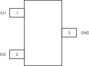
GUID-597BD570-CAE4-4644-8421-BDB7742971E8-low.gif Figure 5-2 DCK Package,3-Pin SC70(Top View)
Table 5-1 Pin Functions
PIN TYPE(1) DESCRIPTION
NAME NO.
IO1 1 I/O The IO1 and IO2 pins are an ESD protected channel. Connect these pins to the data line as close to the connector as possible.
IO2 2 I/O
GND 3 G The GND (ground) pin is connected to ground.
I = input, O = output, G = ground