ZHCSF86A March 2016 – June 2016 TPD1E0B04
PRODUCTION DATA.
- 1 特性
- 2 应用
- 3 说明
- 4 修订历史记录
- 5 Pin Configuration and Functions
- 6 Specifications
-
7 Detailed Description
- 7.1 Overview
- 7.2 Functional Block Diagram
- 7.3
Feature Description
- 7.3.1 IEC 61000-4-2 ESD Protection
- 7.3.2 IEC 61000-4-4 EFT Protection
- 7.3.3 IEC 61000-4-5 Surge Protection
- 7.3.4 IO Capacitance
- 7.3.5 DC Breakdown Voltage
- 7.3.6 Ultra Low Leakage Current
- 7.3.7 Low ESD Clamping Voltage
- 7.3.8 Supports High Speed Interfaces
- 7.3.9 Industrial Temperature Range
- 7.3.10 Industry Standard Package
- 7.4 Device Functional Modes
- 8 Application and Implementation
- 9 Power Supply Recommendations
- 10Layout
- 11器件和文档支持
- 12机械、封装和可订购信息
封装选项
机械数据 (封装 | 引脚)
散热焊盘机械数据 (封装 | 引脚)
订购信息
8 Application and Implementation
NOTE
Information in the following applications sections is not part of the TI component specification, and TI does not warrant its accuracy or completeness. TI’s customers are responsible for determining suitability of components for their purposes. Customers should validate and test their design implementation to confirm system functionality.
8.1 Application Information
The TPD1E0B04 is a diode type TVS which is used to provide a path to ground for dissipating ESD events on high-speed signal lines between a human interface connector and a system. As the current from ESD passes through the TVS, only a small voltage drop is present across the diode. This is the voltage presented to the protected IC. The low RDYN of the triggered TVS holds this voltage, VCLAMP, to a safe level for the protected IC.
8.2 Typical Applications
8.2.1 USB Type-C Application
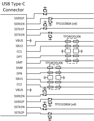 Figure 13. USB Type-C for Thunderbolt 3 ESD Schematic
8.2.1.1 Design Requirements
For this design example eight TPD1E0B04 devices and two TPD4E05U06 devices are being used in a USB Type-C for Thunderbolt 3 application. This provides a complete ESD protection scheme.
Given the Thunderbolt 3 application, the parameters listed in Table 1 are known.
Table 1. Design Parameters
| DESIGN PARAMETER | VALUE |
|---|---|
| Signal range on superspeed Lines | 0 V to 3.6 V |
| Operating frequency on superspeed Lines | up to 10 GHz |
| Signal range on CC, SBU, and DP/DM Lines | 0 V to 5 V |
| Operating frequency on CC, SBU, and DP/DM Lines | up to 480 MHz |
8.2.1.2 Detailed Design Procedure
8.2.1.2.1 Signal Range
The TPD1E0B04 supports signal ranges between –3.6 V and 3.6 V, which supports the SuperSpeed pairs on the USB Type-C application. The TPD4E05U06 supports signal ranges between 0 V and 5.5 V, which supports the CC, SBU, and DP-DM lines.
8.2.1.2.2 Operating Frequency
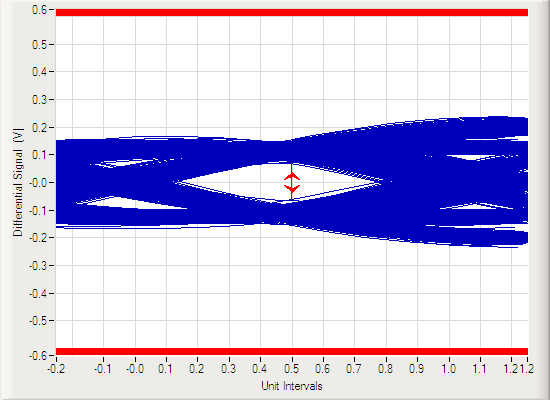
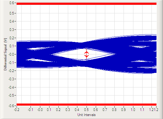
The TPD1E0B04 has a 0.13 pF (typical) capacitance, which supports the Thunderbolt 3 data rates of 20 Gbps. The TPD4E05U06 has a 0.5-pF (typical) capacitance, which easily supports the CC, SBU, and DP-DM data rates.
8.2.1.3 Application Curves

8.2.2 WiFi Antenna Application
 Figure 17. WiFi Antenna Schematic
8.2.2.1 Design Requirements
For this design example one TPD1E0B04 device for a 5-GHz WiFi antenna application. This provides a complete ESD protection scheme.
Given the WiFi antenna application, the parameters listed in Table 2 are known.
Table 2. Design Parameters
| DESIGN PARAMETER | VALUE |
|---|---|
| Signal range | –3.16 V to +3.16 V |
| Operating frequency | 5.170 GHz to 5.835 GHz |
8.2.2.2 Detailed Design Procedure
8.2.2.2.1 Signal Range
The TPD1E0B04 supports signal ranges between –3.6 V and 3.6 V, which supports the antenna signal range. The signal range shown assumes maximum transmit power of 200 mW into a 50-Ω antenna.
8.2.2.2.2 Operating Frequency
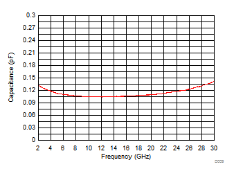
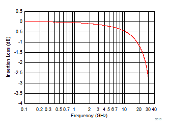
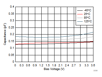
The TPD1E0B04 has a 0.13 pF (typical) capacitance, which supports extremely high data rates. The capacitance vs. frequency and bias voltages are exceedingly low, allowing for very low RF loss and known impedance characteristics. Since capacitance and loss changes very little across the operating frequencies, there must be minimal disturbance on the line.
8.2.2.3 Application Curves
