ZHCSF86A March 2016 – June 2016 TPD1E0B04
PRODUCTION DATA.
- 1 特性
- 2 应用
- 3 说明
- 4 修订历史记录
- 5 Pin Configuration and Functions
- 6 Specifications
-
7 Detailed Description
- 7.1 Overview
- 7.2 Functional Block Diagram
- 7.3
Feature Description
- 7.3.1 IEC 61000-4-2 ESD Protection
- 7.3.2 IEC 61000-4-4 EFT Protection
- 7.3.3 IEC 61000-4-5 Surge Protection
- 7.3.4 IO Capacitance
- 7.3.5 DC Breakdown Voltage
- 7.3.6 Ultra Low Leakage Current
- 7.3.7 Low ESD Clamping Voltage
- 7.3.8 Supports High Speed Interfaces
- 7.3.9 Industrial Temperature Range
- 7.3.10 Industry Standard Package
- 7.4 Device Functional Modes
- 8 Application and Implementation
- 9 Power Supply Recommendations
- 10Layout
- 11器件和文档支持
- 12机械、封装和可订购信息
封装选项
机械数据 (封装 | 引脚)
散热焊盘机械数据 (封装 | 引脚)
订购信息
7 Detailed Description
7.1 Overview
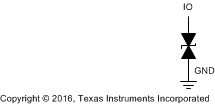
The TPD1E0B04 device is a bidirectional ESD Protection Diode with ultra-low capacitance. This device can dissipate ESD strikes at the maximum level specified by the IEC 61000-4-2 International Standard (contact). The ultra-low capacitance makes this device ideal for protecting any super high-speed signal pins including Thunderbolt 3. The low capacitance allows for extremely low losses even at RF frequencies such as USB 3.1 Gen 2, Thunderbolt 3, or antenna applications.
7.2 Functional Block Diagram

7.3 Feature Description
7.3.1 IEC 61000-4-2 ESD Protection
The I/O pins can withstand ESD events up to ±8-kV contact and ±9-kV air gap. An ESD-surge clamp diverts the current to ground.
7.3.2 IEC 61000-4-4 EFT Protection
The I/O pins can withstand an electrical fast transient burst of up to 80 A (5/50 ns waveform, 4 kV with 50-Ω impedance). An ESD-surge clamp diverts the current to ground.
7.3.3 IEC 61000-4-5 Surge Protection
The I/O pins can withstand surge events up to 1.7 A and 15 W (8/20 µs waveform). An ESD-surge clamp diverts this current to ground.
7.3.4 IO Capacitance
The capacitance between each I/O pin to ground is 0.13 pF (typical) and 0.15 pF (maximum). This device supports data rates in excess of 20 Gbps.
7.3.5 DC Breakdown Voltage
The DC breakdown voltage of each I/O pin is ±6.7 V (typical). This ensures that sensitive equipment is protected from surges above the reverse standoff voltage of ±3.6 V.
7.3.6 Ultra Low Leakage Current
The I/O pins feature an ultra-low leakage current of 10 nA (maximum) with a bias of ±2.5 V
7.3.7 Low ESD Clamping Voltage
The I/O pins feature an ESD clamp that is capable of clamping the voltage to 10.1 V (IPP = 5 A).
7.3.8 Supports High Speed Interfaces
This device is capable of supporting high speed interfaces in excess of 20 Gbps, because of the extremely low IO capacitance.
7.3.9 Industrial Temperature Range
This device features an industrial operating range of –40°C to +125°C.
7.3.10 Industry Standard Package
The layout of this device makes it simple and easy to add protection to an existing layout. The package is offered in industry standard 0201 footprint, requiring minimal modification to an existing layout.
7.4 Device Functional Modes
The TPD1E0B04 device is a passive integrated circuit that triggers when voltages are above VBRF or below VBRR. During ESD events, voltages as high as ±9 kV (air) can be directed to ground via the internal diode network. When the voltages on the protected line fall below the trigger levels of TPD1E0B04 (usually within 10s of nano-seconds) the device reverts to passive.