ZHCSGU7 October 2017 TLV3544-Q1
PRODUCTION DATA.
8 Application and Implementation
NOTE
Information in the following applications sections is not part of the TI component specification, and TI does not warrant its accuracy or completeness. TI’s customers are responsible for determining suitability of components for their purposes. Customers should validate and test their design implementation to confirm system functionality.
8.1 Application Information
The TLV3544-Q1 is a CMOS, rail-to-rail I/O, high-speed, voltage-feedback operational amplifier designed for video, high-speed, and other applications. The amplifier features a 100-MHz gain bandwidth, and 150-V/µs slew rate, but it is unity-gain stable and can be operated as a 1-V/V voltage follower.
8.2 Typical Application
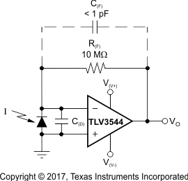
Wide gain bandwidth, low input bias current, low input voltage, and current noise make the TLV3544-Q1 an ideal wideband photodiode transimpedance amplifier. Low-voltage noise is important because photodiode capacitance causes the effective noise gain of the circuit to increase at high frequency. The key elements to a transimpedance design, as shown in Figure 37, are the expected diode capacitance, which include the parasitic input common-mode and differential-mode input capacitance; the desired transimpedance gain; and the gain-bandwidth (GBW) for the TLV3544-Q1 (20 MHz). With these three variables set, the feedback capacitor value can be set to control the frequency response. Feedback capacitance includes the stray capacitance of, which is 0.2 pF for a typical surface-mount resistor.
 Figure 37. Dual-Supply Transimpedance Amplifier
8.2.1 Design Requirements
For this design example, use the parameters listed in Table 2 as the input parameters.
Table 2. Design Parameters
| PARAMETER | EXAMPLE VALUE |
|---|---|
| Supply voltage, V(V+) | 2.5 V |
| Supply voltage, V(V-) | –2.5 V |
C(F) is optional to prevent gain peaking. C(F) includes the stray capacitance of R(F).
8.2.2 Detailed Design Procedure
To achieve a maximally-flat, second-order Butterworth frequency response, set the feedback pole using Equation 3.

Calculate the bandwidth using Equation 4.

8.2.2.1 Optimizing the Transimpedance Circuit
To achieve the best performance, components must be selected according to the following guidelines:
1. For lowest noise, select R(F) to create the total required gain. Using a lower value for R(F) and adding gain after the transimpedance amplifier generally produces poorer noise performance. The noise produced by R(F) increases with the square-root of R(F), whereas the signal increases linearly. Therefore, signal-to-noise ratio improves when all the required gain is placed in the transimpedance stage.
2. Minimize photodiode capacitance and stray capacitance at the summing junction (inverting input). This capacitance causes the voltage noise of the op amp to be amplified (increasing amplification at high frequency). Using a low-noise voltage source to reverse-bias a photodiode can significantly reduce the capacitance. Smaller photodiodes have lower capacitance. Use optics to concentrate light on a small photodiode.
3. Noise increases with increased bandwidth. Limit the circuit bandwidth to only that required. Use a capacitor across the R(F) to limit bandwidth, even if not required for stability.
4. Circuit board leakage can degrade the performance of an otherwise well-designed amplifier. Clean the circuit board carefully. A circuit board guard trace that encircles the summing junction and is driven at the same voltage can help control leakage.
8.2.3 Application Curve
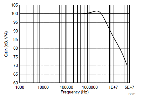
 Figure 38. AC Transfer Function