ZHCSGU7 October 2017 TLV3544-Q1
PRODUCTION DATA.
6 Specifications
6.1 Absolute Maximum Ratings
over operating free-air temperature range (unless otherwise noted)(1)| MIN | MAX | UNIT | ||
|---|---|---|---|---|
| Voltage | Supply voltage, V+ to V− | 7.5 | V | |
| Signal input terminals(2) | (V−) − (0.5) | (V+) + 0.5 | ||
| Current | Signal input terminals(2) | –10 | 10 | mA |
| Output short circuit(3) | Continuous | |||
| Temperature | Operating, TA | –55 | 150 | °C |
| Junction, TJ | 150 | |||
| Storage, Tstg | –65 | 150 | ||
(1) Stresses beyond those listed under Absolute Maximum Ratings may cause permanent damage to the device. These are stress ratings only, which do not imply functional operation of the device at these or any other conditions beyond those indicated under Recommended Operating Conditions. Exposure to absolute-maximum-rated conditions for extended periods may affect device reliability.
(2) Input pins are diode-clamped to the power-supply rails. Input signals that can swing more than 0.5 V beyond the supply rails must be current limited to 10 mA or less.
(3) Short-circuit to ground, one amplifier per package.
6.2 ESD Ratings
| VALUE | UNIT | |||
|---|---|---|---|---|
| V(ESD) | Electrostatic discharge | Human-body model (HBM), per AEC Q100-002(1) | ±1000 | V |
| Charged-device model (CDM), per AEC Q100-011 | ±250 | |||
(1) AEC Q100-002 indicates that HBM stressing shall be in accordance with the ANSI/ESDA/JEDEC JS-001 specification.
6.3 Recommended Operating Conditions
over operating free-air temperature range (unless otherwise noted)| MIN | MAX | UNIT | ||
|---|---|---|---|---|
| VS | Supply voltage, V– to V+ | 2.5 | 5.5 | V |
| Specified temperature | –40 | 125 | °C | |
6.4 Thermal Information: TLV3544-Q1
| THERMAL METRIC | TLV3544-Q1 | UNIT | ||
|---|---|---|---|---|
| PW (TSSOP) | ||||
| 14 PINS | ||||
| RθJA | Junction-to-ambient thermal resistance | 92.6 | °C/W | |
| RθJC(top) | Junction-to-case (top) thermal resistance | 27.5 | °C/W | |
| RθJB | Junction-to-board thermal resistance | 33.6 | °C/W | |
| ψJT | Junction-to-top characterization parameter | 1.9 | °C/W | |
| ψJB | Junction-to-board characterization parameter | 33.1 | °C/W | |
| RθJC(bot) | Junction-to-case (bottom) thermal resistance | — | °C/W | |
6.5 Electrical Characteristics: VS = 2.7 V to 5.5 V Single-Supply
At TA = 25°C, RF = 0 Ω, RL = 1 kΩ, and connected to VS/2, unless otherwise noted.| PARAMETER | TEST CONDITIONS | MIN | TYP | MAX | UNIT | ||
|---|---|---|---|---|---|---|---|
| OFFSET VOLTAGE | |||||||
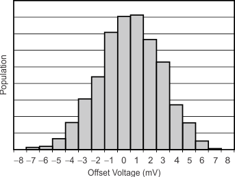
| VOS | Input offset voltage | VS = 5 V, at TA = 25°C | ±2 | ±10 | mV | ||
| dVOS/dT | Input offset voltage vs temperature | VS = 5 V, at TA = −40°C to +125°C | ±4.5 | µV/°C | |||
| PSRR | Input offset voltage vs power supply | VS = 2.7 V to 5.5 V, VCM = (VS/2) − 0.55 V |
±200 | ±800 | µV/V | ||
| VS = 2.7 V to 5.5 V, VCM = (VS/2) − 0.55 V, at TA = −40°C to +125°C |
±900 | ||||||
| INPUT BIAS CURRENT | |||||||
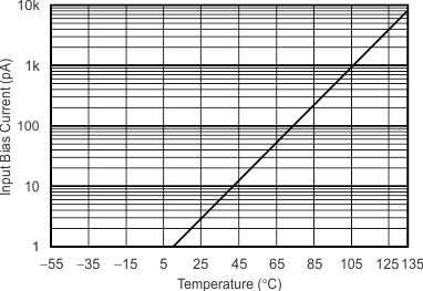
| IB | Input bias current | 3 | pA | ||||
| IOS | Input offset current | ±1 | pA | ||||
| NOISE | |||||||
| en | Input voltage noise density | f = 1 MHz | 7.5 | nV/√Hz | |||
| in | Current noise density | f = 1 MHz | 50 | fA/√Hz | |||
| INPUT VOLTAGE RANGE | |||||||
| VCM | Common-mode voltage | (V−) − 0.1 | (V+) + 0.1 | V | |||
| CMRR | Common-mode rejection ratio | VS = 5.5 V, –0.1 V < VCM < 3.5 V, at TA = 25°C |
66 | 80 | dB | ||
| VS = 5.5 V, –0.1 V < VCM < 5.6 V, at TA = 25°C |
56 | 68 | |||||
| INPUT IMPEDANCE | |||||||
| Differential | 1013 || 2 | Ω || pF | |||||
| Common-mode | 1013 || 2 | Ω || pF | |||||
| OPEN-LOOP GAIN | |||||||
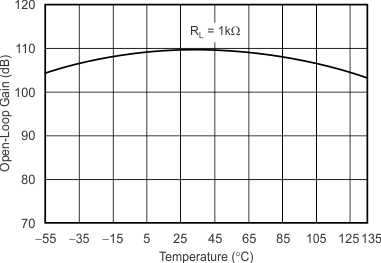
| AOL | Open-loop gain | VS = 5.5 V, 0.3 V < VO < 4.7 V, at TA = 25°C |
94 | 110 | dB | ||
| VS = 5 V, 0.4 V < VO < 4.6 V, at TA = –40°C to +125°C |
90 | ||||||
| FREQUENCY RESPONSE | |||||||
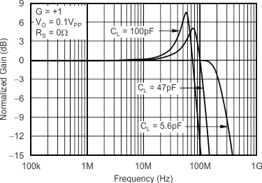
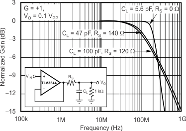
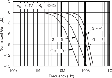
| f−3dB | Small-signal bandwidth | At G = +1, VO = 100 mVPP, RF = 25 Ω |
250 | MHz | |||
| At G = +2, VO = 100 mVPP | 90 | ||||||
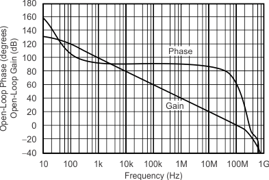
| GBW | Gain-bandwidth product | G = +10 | 100 | MHz | |||
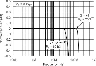
| f0.1dB | Bandwidth for 0.1-dB gain flatness | At G = +2, VO = 100 mVPP | 40 | MHz | |||
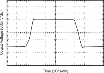
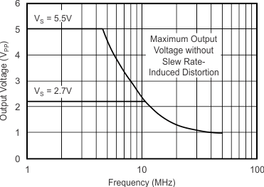
| SR | Slew rate | VS = 5 V, G = +1, 4-V step | 150 | V/µs | |||
| VS = 5 V, G = +1, 2-V step | 130 | ||||||
| VS = 3 V, G = +1, 2-V step | 110 | ||||||
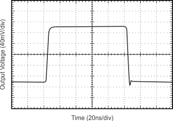
| Rise-and-fall time | At G = +1, VO = 200 mVPP, 10% to 90% |
2 | ns | ||||
| At G = +1, VO = 2 VPP, 10% to 90% | 11 | ||||||
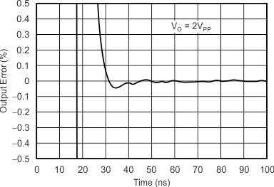
| Settling time | 0.1%, VS = 5 V, G = +1, 2-V output step |
30 | ns | ||||
| 0.01%, VS = 5 V, G = +1, 2-V output step |
60 | ||||||
| Overload recovery time | VIN × Gain = VS | 5 | ns | ||||
| FREQUENCY RESPONSE, continued | |||||||
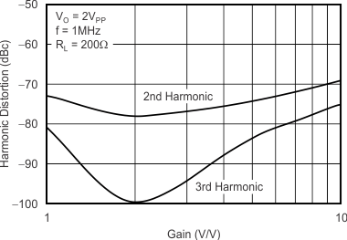
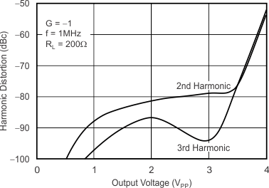
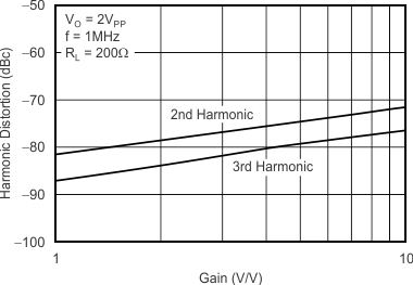
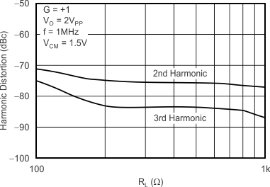
| Harmonic distortion | Second harmonic | At G = +1, f = 1 MHz, VO = 2 VPP, RL = 200 Ω, VCM = 1.5 V |
–75 | dBc | |||
| Third harmonic | At G = +1, f = 1 MHz, VO = 2 VPP, RL = 200 Ω, VCM = 1.5 V |
–83 | |||||
| Differential gain error | NTSC, RL = 150 Ω | 0.02% | |||||
| Differential phase error | NTSC, RL = 150 Ω | 0.09 | ° | ||||
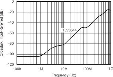
| Channel-to-channel crosstalk | TLV3544-Q1 | f = 5 MHz | –84 | dB | |||
| OUTPUT | |||||||
| Voltage output swing from rail | VS = 5 V, RL = 1 kΩ, AOL > 94 dB, at TA = 25°C |
0.1 | 0.3 | V | |||
| IO | Output current(1)(2) | VS = 5 V | 100 | mA | |||
| VS = 3 V | 50 | mA | |||||
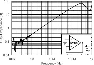
| Closed-loop output impedance | f < 100 kHz | 0.05 | Ω | ||||
| RO | Open-loop output resistance | 35 | Ω | ||||
| POWER SUPPLY | |||||||
| VS | Specified voltage | 2.7 | 5 | V | |||
| Operating voltage | 2.5 | 5.5 | |||||
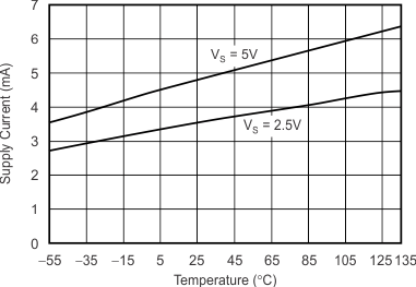
| IQ | Quiescent current (per amplifier) | At TA = 25°C, VS = 5 V, enabled, IO = 0 |
5.2 | 6.5 | mA | ||
| THERMAL SHUTDOWN – JUNCTION TEMPERATURE | |||||||
| Shutdown | 160 | °C | |||||
| Reset from shutdown | 140 | °C | |||||
| THERMAL RANGE | |||||||
| Specified | –40 | 125 | °C | ||||
| Operating | –55 | 150 | °C | ||||
| Storage | –65 | 150 | °C | ||||
(1) See typical characteristic curves, Output Voltage Swing vs Output Current (Figure 20 and Figure 22).
(2) Specified by design.
6.6 Typical Characteristics
At TA = 25°C, VS = 5 V, G = +1, RF = 0 Ω, RL = 1 kΩ, and connected to VS/2, unless otherwise noted.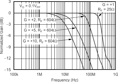
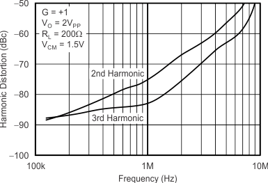
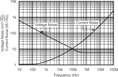
Spectral Density vs Frequency
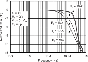
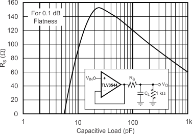
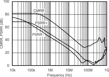
Power-Supply Rejection Ratio vs Frequency
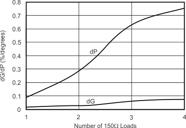
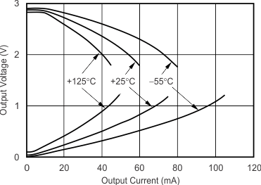
VS = 3 V
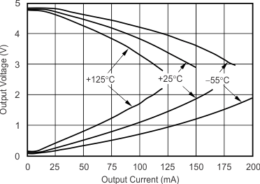
VS = 5 V
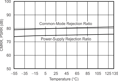
Power-Supply Rejection Ratio vs Temperature