ZHCSGU7 October 2017 TLV3544-Q1
PRODUCTION DATA.
10 Layout
10.1 Layout Guidelines
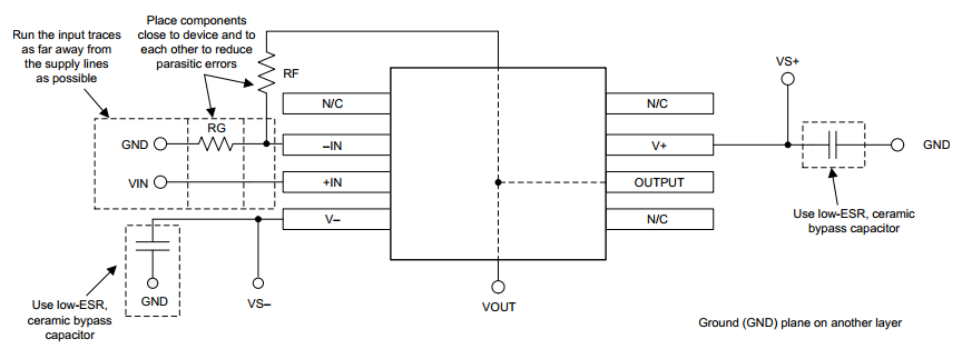
Good high-frequency printed-circuit board (PCB) layout techniques must be employed for the TLV3544-Q1. Generous use of ground planes, short and direct signal traces, and a suitable bypass capacitor located at the V+ pin assure clean, stable operation. Large areas of copper also provides a means of dissipating heat that is generated in normal operation.
TI does not recommend using sockets with any high-speed amplifier.
A 10-nF ceramic bypass capacitor is the minimum recommended value; adding a 1-µF or larger tantalum capacitor in parallel can be beneficial when driving a low-resistance load. Providing adequate bypass capacitance is essential to achieving very low harmonic and intermodulation distortion.
10.2 Layout Example
 Figure 39. Operational Amplifier Board Layout for Noninverting Configuration
10.3 Power Dissipation
Power dissipation depends on power-supply voltage, signal and load conditions. With DC signals, power dissipation is equal to the product of output current times the voltage across the conducting output transistor,
VS − VO. Power dissipation can be minimized by using the lowest possible power-supply voltage necessary to assure the required output voltage swing.
For resistive loads, the maximum power dissipation occurs at a DC output voltage of one-half the power-supply voltage. Dissipation with AC signals is lower. AB-039 Power Amplifier Stress and Power Handling Limitations explains how to calculate or measure power dissipation with unusual signals and loads, and can be found at www.ti.com.
Any tendency to activate the thermal protection circuit indicates excessive power dissipation or an inadequate heatsink. For reliable operation, junction temperature must be limited to 150°C, maximum. To estimate the margin of safety in a complete design, increase the ambient temperature until the thermal protection is triggered at 160°C. The thermal protection should trigger more than 35°C above the maximum expected ambient condition of the application.