ZHCSK03J August 1983 – November 2023 TLC555
PRODUCTION DATA
- 1
- 1 特性
- 2 应用
- 3 说明
- 4 Pin Configuration and Functions
-
5 Specifications
- 5.1 Absolute Maximum Ratings
- 5.2 ESD Ratings
- 5.3 Recommended Operating Conditions
- 5.4 Thermal Information
- 5.5 Electrical Characteristics: VDD = 2 V for TLC555C, VDD = 3 V for TLC555I
- 5.6 Electrical Characteristics: VDD = 5 V
- 5.7 Electrical Characteristics: VDD = 15 V
- 5.8 Timing Characteristics
- 5.9 Typical Characteristics
- 6 Detailed Description
- 7 Application and Implementation
- 8 Device and Documentation Support
- 9 Revision History
- 10Mechanical, Packaging, and Orderable Information
封装选项
机械数据 (封装 | 引脚)
散热焊盘机械数据 (封装 | 引脚)
订购信息
7.2.5 Designing for Improved ESD Performance
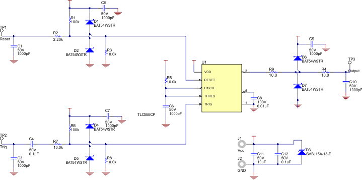
The TLC555 internal HBM and CDM protection allows for safe assembly in ESD-controlled environments. In applications that expose the pins of the TLC555 to ESD, additional protection is highly recommended. The following test board schematic has bypass capacitors, current-limiting resistors, and voltage-clamping TVS diodes to provide additional protection for commonly exposed pins (Reset, Trig, and Output) against ESD.
 Figure 7-10 ESD
Test Schematic
Figure 7-10 ESD
Test SchematicThe following table gives the ESD protection levels recorded for different supply voltages and external components populated. Using only passive components to protect the TLC555 with a single 15‑V supply is not recommended because the higher voltage allows for an unacceptable amount of current to flow through the device.
| SUPPLY VOLTAGE | ONLY PASSIVE COMPONENTS
POPULATED D1..D7 NOT POPULATED(1) |
ALL COMPONENTS POPULATED (1) |
|---|---|---|
| 5 V | 8 kV | 12 kV |
| 15 V | Not recommended | 12 kV |