ZHCSK03J August   1983  – November 2023 TLC555

PRODUCTION DATA  

  1.   1
  2. 特性
  3. 应用
  4. 说明
  5. Pin Configuration and Functions
  6. Specifications
    1. 5.1 Absolute Maximum Ratings
    2. 5.2 ESD Ratings
    3. 5.3 Recommended Operating Conditions
    4. 5.4 Thermal Information
    5. 5.5 Electrical Characteristics: VDD = 2 V for TLC555C, VDD = 3 V for TLC555I
    6. 5.6 Electrical Characteristics: VDD = 5 V
    7. 5.7 Electrical Characteristics: VDD = 15 V
    8. 5.8 Timing Characteristics
    9. 5.9 Typical Characteristics
  7. Detailed Description
    1. 6.1 Overview
    2. 6.2 Functional Block Diagram
    3. 6.3 Feature Description
      1. 6.3.1 Monostable Operation
      2. 6.3.2 Astable Operation
      3. 6.3.3 Frequency Divider
    4. 6.4 Device Functional Modes
  8. Application and Implementation
    1. 7.1 Application Information
    2. 7.2 Typical Applications
      1. 7.2.1 Missing-Pulse Detector
        1. 7.2.1.1 Design Requirements
        2. 7.2.1.2 Detailed Design Procedure
        3. 7.2.1.3 Application Curve
      2. 7.2.2 Pulse-Width Modulation
        1. 7.2.2.1 Design Requirements
        2. 7.2.2.2 Detailed Design Procedure
        3. 7.2.2.3 Application Curve
      3. 7.2.3 Pulse-Position Modulation
        1. 7.2.3.1 Design Requirements
        2. 7.2.3.2 Detailed Design Procedure
        3. 7.2.3.3 Application Curves
      4. 7.2.4 Sequential Timer
        1. 7.2.4.1 Design Requirements
        2. 7.2.4.2 Detailed Design Procedure
        3. 7.2.4.3 Application Curve
      5. 7.2.5 Designing for Improved ESD Performance
    3. 7.3 Power Supply Recommendations
    4. 7.4 Layout
      1. 7.4.1 Layout Guidelines
      2. 7.4.2 Layout Example
  9. Device and Documentation Support
    1. 8.1 接收文档更新通知
    2. 8.2 支持资源
    3. 8.3 Trademarks
    4. 8.4 静电放电警告
    5. 8.5 术语表
  10. Revision History
  11. 10Mechanical, Packaging, and Orderable Information

封装选项

机械数据 (封装 | 引脚)
散热焊盘机械数据 (封装 | 引脚)
订购信息

Frequency Divider

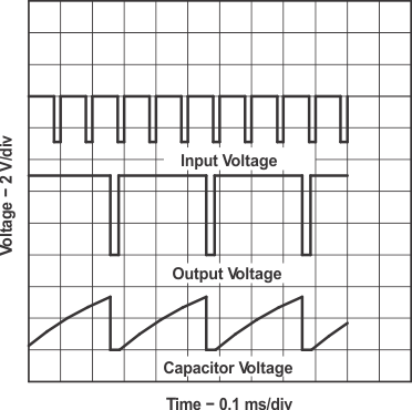
By adjusting the length of the timing cycle, the basic circuit of Figure 6-2 can be made to operate as a frequency divider. Figure 6-9 shows a divide-by-three circuit that makes use of the fact that retriggering cannot occur during the timing cycle.
GUID-E8CA6085-4340-4DAB-84AA-F1807234B8E7-low.gif
VCC = 5 V RA = 1250 Ω C = 0.02 µF
See Figure 6-2
Figure 6-9 Divide-by-Three Circuit Waveforms