ZHCSAH8B November   2012  – March 2022 TFP401A-Q1

PRODUCTION DATA  

  1. 特性
  2. 应用
  3. 说明
  4. Revision History
  5. Pin Configuration and Functions
  6. Specifications
    1. 6.1  Absolute Maximum Ratings
    2. 6.2  ESD Ratings
    3. 6.3  Recommended Operating Conditions
    4. 6.4  Thermal Information
    5. 6.5  DC Digital I/O Electrical Characteristics
    6. 6.6  DC Electrical Characteristics
    7. 6.7  AC Electrical Characteristics
    8. 6.8  Timing Requirements
    9. 6.9  Switching Characteristics
    10. 6.10 Typical Characteristics
  7. Detailed Description
    1. 7.1 Overview
    2. 7.2 Functional Block Diagram
    3. 7.3 Feature Description
      1. 7.3.1 TMDS Pixel Data and Control Signal Encoding
      2. 7.3.2 TFP401A-Q1 Clocking and Data Synchronization
      3. 7.3.3 TFP401A-Q1 TMDS Input Levels and Input Impedance Matching
      4. 7.3.4 TFP401A-Q1 Device Incorporates HSYNC Jitter Immunity
    4. 7.4 Device Functional Modes
      1. 7.4.1 TFP401A-Q1 Modes of Operation
      2. 7.4.2 TFP401A-Q1 Output Driver Configurations
  8. Application and Implementation
    1. 8.1 Application Information
      1. 8.1.1 Typical Application
        1. 8.1.1.1 Design Requirements
        2. 8.1.1.2 Detailed Design Procedure
          1. 8.1.1.2.1 Data and Control Signals
          2. 8.1.1.2.2 Configuration Options
          3. 8.1.1.2.3 Power Supplies Decoupling
        3. 8.1.1.3 Application Curves
        4. 8.1.1.4 DVDD
        5. 8.1.1.5 OVDD
        6. 8.1.1.6 AVDD
        7. 8.1.1.7 PVDD
    2. 8.2 Power Supply Recommendations
    3. 8.3 Layout
      1. 8.3.1 Layout Guidelines
        1. 8.3.1.1 Layer Stack
        2. 8.3.1.2 Routing High-Speed Differential Signal Traces (RxC-, RxC+, Rx0-, Rx0+, Rx1-, Rx1+, Rx2-, Rx2+)
      2. 8.3.2 Layout Example
      3. 8.3.3 TI PowerPAD 100-TQFP Package
  9. Device and Documentation Support
    1. 9.1 接收文档更新通知
    2. 9.2 支持资源
    3. 9.3 Trademarks
    4. 9.4 Electrostatic Discharge Caution
    5. 9.5 术语表
  10. 10Mechanical, Packaging, and Orderable Information

封装选项

机械数据 (封装 | 引脚)
散热焊盘机械数据 (封装 | 引脚)
订购信息

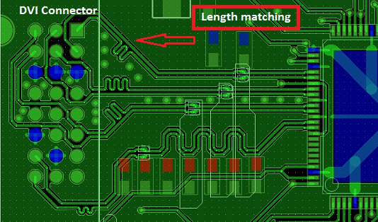
Layout Example

  • DVI connector trace matching
    GUID-48A35B51-D011-425C-A517-9E53F55E9A8D-low.pngFigure 8-8 DVI Connector
  • Keep data lines as far as possible from each other
    GUID-2DA0BD57-FD6B-4252-80D2-BEEB38191228-low.pngFigure 8-9 Data Route
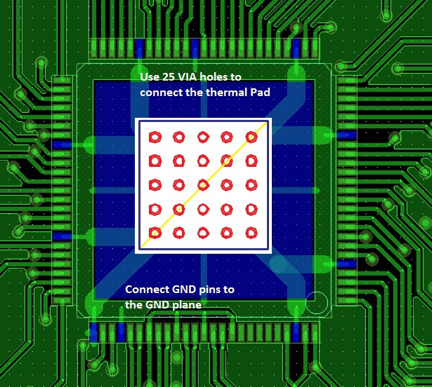
  • Connect the thermal pad to ground
    GUID-091CFF69-CE5C-4562-996D-E55EB90E4175-low.pngFigure 8-10 GND Route