SLLSE81A March 2011 – March 2016 SN75LVCP600S
PRODUCTION DATA.
- 1 Features
- 2 Applications
- 3 Description
- 4 Revision History
- 5 Pin Configuration and Functions
- 6 Specifications
- 7 Parameter Measurement Information
- 8 Detailed Description
- 9 Application and Implementation
- 10Power Supply Recommendations
- 11Layout
- 12Device and Documentation Support
- 13Mechanical, Packaging, and Orderable Information
8 Detailed Description
8.1 Overview
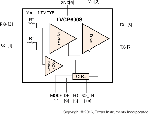
The SN75LVCP600S is a single-channel SATA/SAS signal conditioner supporting data rates up to 6 Gbps with an extended temperature range from –40°C to 85°C. The device complies with SATA physical spec rev 3.0 and SAS electrical spec 2.0. The SN75LVCP600S operates from a single 3.3-V supply and has 100-Ω line termination with a self-biasing feature, making the device suitable for AC coupling. The inputs incorporate an out-of-band (OOB) detector, which automatically squelches the output while maintaining a stable common-mode voltage compliant to the SATA/SAS link.
The SN75LVCP600S handles interconnect losses at its input with selectable equalization settings that can be programmed to the match loss in the channel. For data rates of 3 Gbps and lower, the LVCP600S equalizes signals for a span of up to 50 inches of FR4 board material. For data rates of 6 Gbps, the device compensates >40 inches (1 m) of FR4 material. Rx/Tx equalization level is controlled by the setting of signal control pins EQ and DE.
The device is hot-plug capable, preventing device damage during device hot-insertion such as async signal plug/removal, unpowered plug/removal, powered plug/removal, or surprise plug/removal.
8.2 Functional Block Diagram

8.3 Feature Description
8.3.1 Input Equalization
The SN75LVCP600S supports programmable equalization in its front stage; the equalization settings are shown in Table 1. The input equalizer is designed to recover a signal even when no eye is present at the receiver and effectively supports FR4 trace at the input anywhere from 4 inches (0.1 m) to 40 (1 m) at SATA 6-Gbps speed. In SAS mode, the device meets compliance point IR in a TX/RX connection.
 Figure 11. Compliance Point In SAS Mode
8.3.2 Auto Low-Power (ALP) Mode (see Figure 5)
As a redriver, the SN75LVCP600S does not participate in SATA or SAS link power management (PM) states. However, the redriver tracks link-power management mode (partial and slumber) by relying on the link differential voltage, VIDp-p. The SATA/SAS link is continuously sending and receiving data even in long periods of disk inactivity by sending SYNC primitives (logical idle), except when the link enters partial or slumber mode. In these modes, the link is in an electrical-idle state (EID). The device input squelch detector tracks EID status. When the input signal is in the electrical idle state, that is, VIDp-p <VOOB_SATA/VOOB_SAS and stays in this state for > 10 µS, the device automatically enters the low power state. In this state, the output is driven to VCM and the device selectively shuts off internal circuitry to lower power consumption by approximately 90% of its normal operating power. While in ALP mode, the device continues to monitor input signal levels actively; when the input signal exceeds the SATA/SAS OOB upper threshold level, the device reverts to the active state. Exit time from auto low-power mode is <50 ns (maximum).
8.3.3 Out-Of-Band (OOB) Support
The squelch detector circuit within the device enables full detection of OOB signaling as specified in the SATA and SAS specifications. Selection of squelch threshold level is made automatically based on the state of MODE pin, SATA or SAS. Squelch circuit ON/OFF time is 8 ns maximum. While in squelch mode, outputs are held to VCM.
8.4 Device Functional Modes
Table 1. EQ and DE Settings
| LEVEL | CONTROL PINS | |||
|---|---|---|---|---|
| EQ (TYP) dB at 6 Gbps |
DE (TYP) dB at 6 Gbps |
SQ_TH (SEE VOOB SPEC) | MODE | |
| 0 (default) | 7 | 0 | Full level (normal) | SATA |
| 1 | 14 | –1.3 | Reduced level (long channel) | SAS |
Trace lengths are suggested values based on TI spice simulations (done over programmable limits of input EQ) to meet SATA/SAS loss and jitter spec.
Actual trace length supported by the LVCP600S may be more or less than suggested values and depends on board layout, trace widths, and number of connectors used in the high-speed signal path. See the Application Curves for more placement guidance
 Figure 12. Trace Length Example