ZHCSCJ4A February 2014 – October 2014 SN74GTL2014
PRODUCTION DATA.
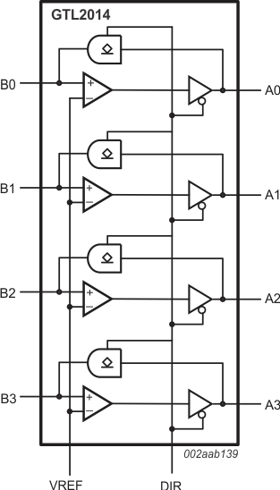
8 Detailed Description
8.1 Overview
The GTL2014 is a 4-channel translating transceiver designed for 3.3-V LVTTL system interface with a GTL–/GTL/GTL+ bus, where GTL–/GTL/GTL+ refers to the reference voltage of the GTL bus and the input/output voltage thresholds associated with it.
The direction pin allows the part to function as either a GTL-to-LVTTL sampling receiver or as a LVTTL-to-GTL interface.
8.2 Functional Block Diagram
8.3 Feature Description
8.3.1 5 V tolerance on LVTTL input
The GTL2014 LVTTL inputs (only) are tolerant up to 5.5 V and allows direct access to TTL or 5 V CMOS inputs. The LVTTL outputs are not 5.5 V tolerant.
8.3.2 3.6 V tolerance on GTL Input/Output
The GTL2014 GTL inputs and outputs operate up to 3.6 V, allowing the device to be used in higher voltage open-drain output applications.
8.3.3 Ultra-Low VREF and High Bandwidth
GTL2014’s VREF tracks down to 0.5 V for low voltage CPUs with excellent propagation delay performance. This feature allows the GTL2014 to support high data rates with the GTL– bus.
8.4 Device Functional Modes
The GTL2014 performs translation in two directions. One direction is GTL–/GTL/GTL+ to LVTTL when DIR is tied to GND. With appropriate VREF set up, the GTL input can be compliant with GTL–/GTL/GTL+. Another direction is LVTTL to GTL–/GTL/GTL+ when DIR is tied to VCC. 3.6 V tolerance on the GTL output allows the GTL outputs to pull up to any voltage level under 3.6 V.