ZHCSCJ4A February 2014 – October 2014 SN74GTL2014
PRODUCTION DATA.
6 Specifications
6.1 Absolute Maximum Ratings
Specified at TA = –40°C to 85°C unless otherwise noted(1)| MIN | MAX | UNIT | |||
|---|---|---|---|---|---|
| VCC | Supply voltage | –0.5 | 4.6 | V | |
| IIK | Input clamping current, VI < 0 V | –50 | mA | ||
| VSEL | Input control voltages SEL(2)(3) | –0.5 | 6 | V | |
| VI | Input voltage | A port | –0.5 | 7 | V |
| B port | –0.5 | 4.6 | |||
| IOK | Control input clamp current, VO < 0 V | –50 | mA | ||
| VO | Output voltage | A port | –0.5 | 7 | V |
| B port | –0.5 | 4.6 | |||
| IOL | Current into any output in the low state | A port | 40 | mA | |
| B port | 80 | ||||
| IOH | Current into any output in the high state | –40 | mA | ||
(1) Stresses beyond those listed under Absolute Maximum Ratings may cause permanent damage to the device. These are stress ratings only and functional operation of the device at these conditions is not implied. Exposure to absolute-maximum-rated conditions for extended periods may affect device reliability.
(2) All voltages are with respect to ground, unless otherwise specified
(3) VI and VO are used to denote specific conditions for VI/O
6.2 Handling Ratings
| MIN | MAX | UNIT | |||
|---|---|---|---|---|---|
| Tstg | Storage temperature range | –55 | 150 | °C | |
| VESD(1) | Human Body Model (HBM), JEDEC: JESD22-A114(2) | All pins | 0 | 2 | kV |
| IEC61000-4-2 contact discharge(3) | All pins | 0 | 1 | ||
(1) Electrostatic discharge (ESD) to measure device sensitivity/immunity to damage caused by assembly line electrostatic discharges into the device.
(2) Level listed above is the passing level per ANSI/ESDA/JEDEC JS-001. JEDEC document JEP155 states that 500-V HBM allows safe manufacturing with a standard ESD control process. Pins listed as 250 V may actually have higher performance.
(3) Level listed above is the passing level per EIA-JEDEC JESD22-C101. JEDEC document JEP157 states that 250-V CDM allows safe manufacturing with a standard ESD control process. Pins listed as 250 V may actually have higher performance.
6.3 Recommended Operating Conditions
over operating free-air temperature range (unless otherwise noted)(1)| MIN | NOM | MAX | UNIT | |||
|---|---|---|---|---|---|---|
| VCC | Supply voltage | 3 | 3.3 | 3.6 | V | |
| VTT | Termination voltage | GTL– | 0.85 | 0.9 | 0.95 | V |
| GTL | 1.14 | 1.2 | 1.26 | |||
| GTL+ | 1.35 | 1.5 | 1.65 | |||
| VREF | Reference voltage | Overall | 0.5 | 2 / 3 VTT | VCC / 2 | V |
| GTL– | 0.5 | 0.6 | 0.63 | |||
| GTL | 0.76 | 0.8 | 0.84 | |||
| GTL+ | 0.87 | 1 | 1.1 | |||
| VI | Input voltage | A port | 0 | 3.3 | 5.5(2) | V |
| B port | 0 | VTT | 3.6 | |||
| VIH | High-level input voltage | A port and DIR | 2 | V | ||
| B port | VREF + 50 mV | |||||
| VIL | Low-level input voltage | A port and DIR | 0.8 | V | ||
| B port | VREF – 50 mV | |||||
| IOH | High-level input current | A port | –20 | mA | ||
| IOL | Low-level output current | A port | 20 | mA | ||
| B port | 50 | |||||
(1) All unused control inputs of the device must be held at VCC or GND to ensure proper device operation. Refer to the TI application report, Implications of Slow or Floating CMOS Inputs, literature number SCBA004.
(2) The VI(max) of LVTTL port is 3.6 V if configured as output (DIR=L)
6.4 Thermal Information
| THERMAL METRIC(1) | SN74GTL2014 | UNIT | |
|---|---|---|---|
| PW | |||
| 14 PINS | |||
| RθJA | Junction-to-ambient thermal resistance | 136.8 | °C/W |
| RθJC(top) | Junction-to-case (top) thermal resistance | 63.0 | |
| RθJB | Junction-to-board thermal resistance | 78.6 | |
| ψJT | Junction-to-top characterization parameter | 11.9 | |
| ψJB | Junction-to-board characterization parameter | 77.9 | |
(1) For more information about traditional and new thermal metrics, see the IC Package Thermal Metrics application report, SPRA953.
6.5 Electrical Characteristics
Specified at TA = –40°C to 85°C (unless otherwise noted)| PARAMETER | TEST CONDITIONS | –40°C TO 85°C | UNIT | |||
|---|---|---|---|---|---|---|
| MIN | TYP | MAX | ||||
| VOH | A port | VCC = 3 to 3.6 V, IOH = –100 µA | VCC – 0.2 | V | ||
| VCC = 3 V, IOH = –16 mA | 2 | |||||
| VOL | A port | VCC = 3 V, IOL = 8 mA | 0.28 | 0.4 | V | |
| A port | VCC = 3 V, IOL = 16 mA | 0.55 | 0.8 | |||
| B port | VCC = 3 V, IOL = 40 mA | 0.23 | 0.4 | |||
| II | A port | VCC = 3.6 V, VI = VCC | ±1 | µA | ||
| VCC = 3.6, VI = 0 V | ±1 | |||||
| VCC = 3.6, VI = 5.5 V | 5 | |||||
| B port | VCC = 3.6 V, VI = VTT or GND | ±1 | µA | |||
| Control pin | VCC = 3.6 V, VI = VCC or 0 V | ±1 | µA | |||
| Ioff | OFF-state output current on A port | VCC = 0 V, VIO = 0 to 3.6 V | ±10 | µA | ||
| OFF-state output current on A port | VCC = 0 V, VIO 3.6 to 5.5V | ±100 | ||||
| OFF-state output current on B port | VCC = 0 V, VIO = 0 to 3.6 V | ±10 | ||||
| ICC | A port | VCC = 3.6 V, VI = VCC or GND, IO = 0 | 3 | 10 | mA | |
| B port | VCC = 3.6 V, VI = VTT or GND, IO = 0 | 3 | 10 | mA | ||
| ∆ICC | A port or control input | VCC = 3.6 V, VI = VCC – 0.6 V | 500 | µA | ||
| CI | Input capacitance of control pin | VI = 3.0 V or 0 V | 2 | 2.5 | pF | |
| CIO | A port | VO = 3 V or 0 | 4 | 6 | pF | |
| B port | VO = VTT or 0 | 5.46 | 5.55 | |||
6.6 Dynamic Electrical Characteristics
over operating range, TA = –40°C to 85°C, VCC = 1.65 to 4.6 V, GND = 0 V for GTL (see Functional Block Diagram)| PARAMETER | GTL− | GTL | GTL+ | UNIT | |||||||
|---|---|---|---|---|---|---|---|---|---|---|---|
| VCC = 3.3 V ± 0.3 V VREF = 0.6 V VTT = 0.9 V |
VCC = 3.3 V ± 0.3 V VREF = 0.8 V VTT = 1.2 V |
VCC = 3.3 V ± 0.3 V VREF = 1 V VTT = 1.5 V |
|||||||||
| MIN | TYP | MAX | MIN | TYP | MAX | MIN | TYP | MAX | |||
| tPLH (low to high propagation delay) | An to Bn | 2.8 | 5 | 2.8 | 5 | 2.8 | 5 | ns | |||
| tPHL(high to low propagation delay) | 3.3 | 7 | 3.4 | 7 | 3.4 | 7 | |||||
| tPLH (low to high propagation delay) | Bn to An | 5.3 | 8 | 5.2 | 8 | 5.1 | 8 | ns | |||
| tPHL (high to low propagation delay) | 5.2 | 8 | 4.9 | 7.16 | 4.7 | 7.16 | |||||
6.7 Typical Characteristics
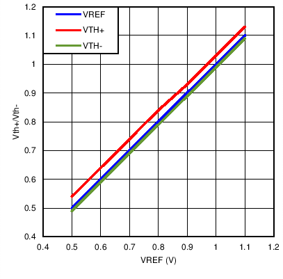 Figure 1. GTL Vth+ and Vth– vs VREF (25°C)
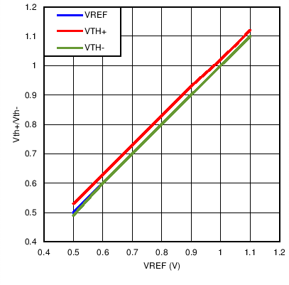 Figure 3. GTL Vth+ and Vth– vs VREF (125°C)
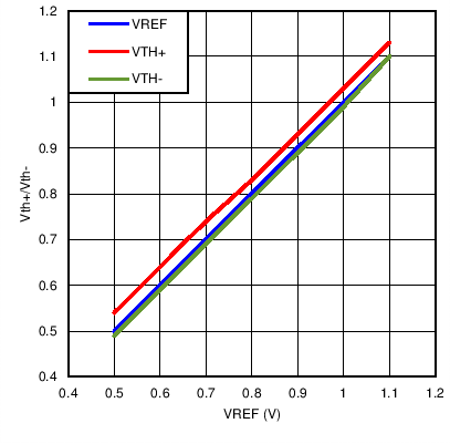 Figure 2. GTL Vth+ and Vth– vs VREF (–40°C)