ZHCSRU4F November 2006 – March 2023 SN65HVD3080E , SN65HVD3083E , SN65HVD3086E
PRODUCTION DATA
- 1 特性
- 2 应用
- 3 说明
- 4 Revision History
-
5 Specifications
- 5.1 Absolute Maximum Ratings
- 5.2 Power Dissipation Ratings
- 5.3 Electrostatic Discharge Protection
- 5.4 Supply Current
- 5.5 Recommended Operating Conditions
- 5.6 Thermal Information
- 5.7 Driver Electrical Characteristics
- 5.8 Driver Switching Characteristics
- 5.9 Receiver Electrical Characteristics
- 5.10 Receiver Switching Characteristics
- 5.11 Typical Characteristics
- 6 Parameter Measurement Information
- 7 Device Information
- 8 Application Information
- 9 Device and Documentation Support
- 10Mechanical, Packaging, and Orderable Information
5.11 Typical Characteristics
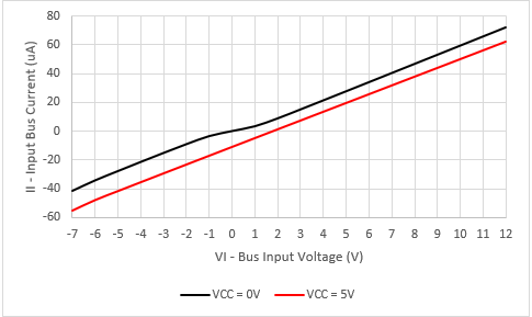 Figure 5-1 Input Bias Current vs BUS Input
Voltage
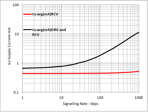 Figure 5-3 HVD3083E Supply Current vs Signaling
Rate
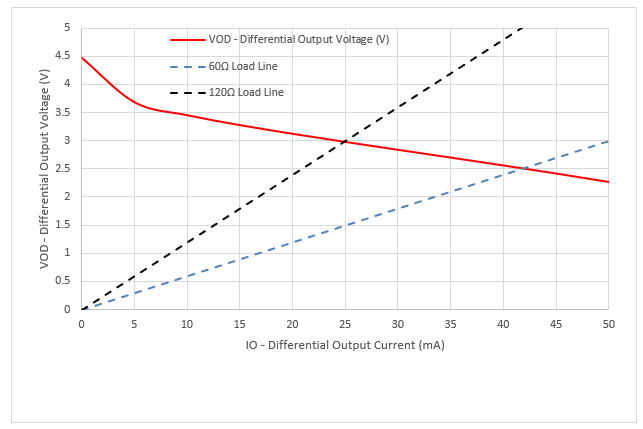 Figure 5-5 Differential Output Voltage vs Differential
Output Current
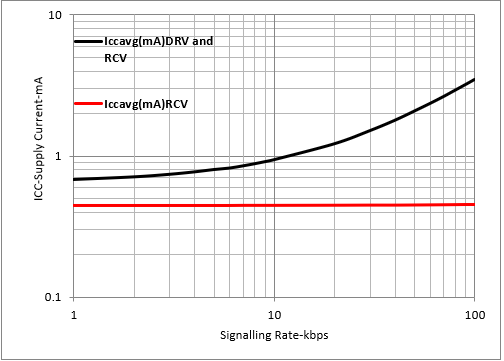 Figure 5-2 HVD3080E Supply Current vs Signaling
Rate
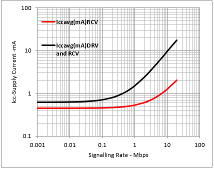 Figure 5-4 HVD3086E Supply Current vs Signaling
Rate
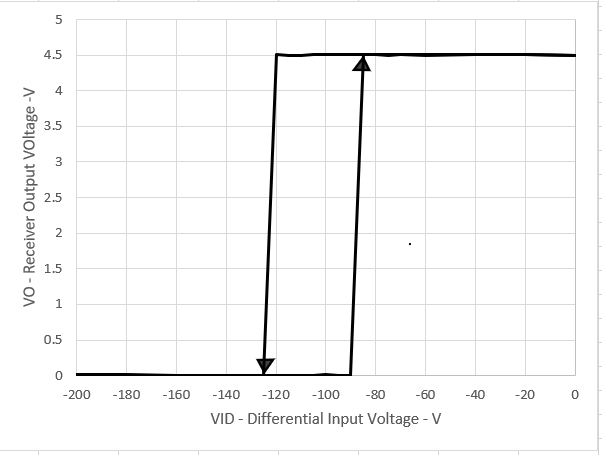 Figure 5-6 Receiver Output Voltage vs Differential Input
Voltage