ZHCSJ17H November 2002 – November 2018 SN65HVD233 , SN65HVD234 , SN65HVD235
PRODUCTION DATA.
- 1 特性
- 2 应用
- 3 说明
- 4 修订历史记录
- 5 (说明 (续))
- 6 Device Comparison Table
- 7 Pin Configuration and Functions
-
8 Specifications
- 8.1 Absolute Maximum Ratings
- 8.2 ESD Ratings
- 8.3 Recommended Operating Conditions
- 8.4 Thermal Information
- 8.5 Power Dissipation Ratings
- 8.6 Electrical Characteristics: Driver
- 8.7 Electrical Characteristics: Receiver
- 8.8 Switching Characteristics: Driver
- 8.9 Switching Characteristics: Receiver
- 8.10 Switching Characteristics: Device
- 8.11 Typical Characteristics
- 9 Parameter Measurement Information
- 10Detailed Description
- 11Application and Implementation
- 12Power Supply Recommendations
- 13Layout
- 14器件和文档支持
- 15机械、封装和可订购信息
11.1 Application Information
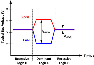
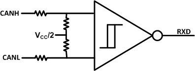
The CAN bus has two states during powered operation of the device; dominant and recessive. A dominant bus state is when the bus is driven differentially, corresponding to a logic low on the D and R pin. A recessive bus state is when the bus is biased to VCC / 2 via the high-resistance internal resistors RIN and RID of the receiver, corresponding to a logic high on the D and R pins. See Figure 34 and Figure 35.
 Figure 34. Bus States (Physical Bit Representation)
  Figure 35. Simplified Recessive Common Mode Bias and Receiver
 These CAN transceivers are typically used in applications with a host microprocessor or FPGA that includes the link layer portion of the CAN protocol. The different nodes on the network are typically connected through the use of a 120-Ω characteristic impedance twisted-pair cable with termination on both ends of the bus.