ZHCSBS4F July 2013 – August 2014 SN65HVD01
PRODUCTION DATA.
6 Specifications
6.1 Absolute Maximum Ratings(1)
| VALUE | UNIT | ||
|---|---|---|---|
| MIN | MAX | ||
| Control supply voltage, VL | –0.5 | 4 | V |
| Bus supply voltage, VCC | –0.5 | 5.5 | V |
| Voltage range at A or B Inputs | –13 | 16.5 | V |
| Input voltage range at any logic terminal | –0.3 | 5.7 | V |
| Voltage input range, transient pulse, A and B, through 100Ω | –100 | 100 | V |
| Receiver output current | –12 | 12 | mA |
| Junction temperature, TJ | 170 | °C | |
| Continuous total power dissipation | See the Thermal Information table | ||
(1) Stresses beyond those listed under "absolute maximum ratings" may cause permanent damage to the device. These are stress ratings only and functional operation of the device at these or any other conditions beyond those indicated under "recommended operating conditions" is not implied. Exposure to absolute-maximum-rated conditions for extended periods may affect device reliability.
6.2 Handling Ratings
| MIN | MAX | UNIT | ||
|---|---|---|---|---|
| TSTG | Storage temperature range | –65 | 150 | °C |
| VESD | IEC 60749-26 ESD (Human Body Model), bus terminals and GND | ±15 | kV | |
| IEC 61000-4-2 ESD (Air-Gap Discharge), bus terminals and GND (1) | ±16 | kV | ||
| IEC 61000-4-2 ESD (Contact Discharge), bus terminals and GND | ±16 | kV | ||
| IEC 61000-4-4 EFT (Fast transient or burst) bus terminals and GND | ±4 | kV | ||
| JEDEC Standard 22, Test Method A114 (Human Body Model), all terminals | ±8 | kV | ||
| JEDEC Standard 22, Test Method C101 (Charged Device Model), all terminals | ±1.5 | kV |
(1) As stated in the IEC 61000-4-2 standard, contact discharge is the preferred transient protection test method. Although IEC air-gap testing is less repeatable than contact testing, air discharge protection levels are inferred from the contact discharge test results.
6.3 Recommended Operating Conditions
| MIN | NOM | MAX | UNIT | |||
|---|---|---|---|---|---|---|
| VL | Control supply voltage | 1.65 | 3.6 | V | ||
| VCC | Bus supply voltage | 3 | 3.3 | 3.6 | V | |
| VI | Input voltage at any bus terminal (separately or common mode) (1) | –7 | 12 | V | ||
| VIH | High-level input voltage (Driver, driver enable, receiver enable inputs, and slew rate select) | 0.7×VL | VL | V | ||
| VIL | Low-level input voltage (Driver, driver enable, receiver enable inputs, and slew rate select) | 0 | 0.3×VL | V | ||
| VID | Differential input voltage | –12 | 12 | V | ||
| IO | Output current | Driver | –80 | 80 | mA | |
| Receiver | –2 | 2 | mA | |||
| RL | Differential load resistance | 54 | 60 | Ω | ||
| CL | Differential load capacitance | 50 | pF | |||
| 1/tUI | Signaling rate | SLR = '0' | 20 | Mbps | ||
| SLR = '1' | 250 | kbps | ||||
| TA(2) | Operating free-air temperature Thermal Information | –40 | 125 | °C | ||
(1) The algebraic convention, in which the least positive (most negative) limit is designated as minimum is used in this data sheet.
(2) Operation is specified for internal (junction) temperatures up to 150°C. Self-heating due to internal power dissipation should be considered for each application. Maximum junction temperature is internally limited by the thermal shut-down (TSD) circuit which disables the driver outputs when the junction temperature reaches 170°C.
6.4 Thermal Information
| PARAMETER(1) | SON (DRC) | UNIT | |
|---|---|---|---|
| ΘJA | Junction-to-Ambient Thermal Resistance | 41.4 | °C/ W |
| ΘJC(top) | Junction-to-Case(top) Thermal Resistance | 48.7 | |
| ΘJB | Junction-to-Board Thermal Resistance | 18.8 | |
| ΨJT | Junction-to-Top characterization parameter | 0.6 | |
| ΨJB | Junction-to-Board characterization parameter | 19 | |
| ΘJC(bottom) | Junction-to-Case(bottom) Thermal Resistance | 3.7 | |
| TTSD | Thermal Shut-down junction temperature | 170 | °C |
(1) For more information about traditional and new thermal metrics, see the IC Package Thermal Metrics application report, SPRA953
6.5 Dissipation Ratings
| PARAMETER | TEST CONDITIONS | VALUE | UNIT | |||
|---|---|---|---|---|---|---|
| PD | Power Dissipation driver and receiver enabled, VCC = VL = 3.6 V, TJ = 150°C, 50% duty cycle square-wave signal at signaling rate |
Unterminated | RL = 300 Ω, CL = 50 pF (driver) |
250 kbps | 125 | mW |
| 20 Mbps | 175 | |||||
| RS-422 load | RL = 100 Ω, CL = 50 pF (driver) |
250 kbps | 165 | mW | ||
| 20 Mbps | 215 | |||||
| RS-485 load | RL = 54 Ω, CL = 50 pF (driver) |
250 kbps | 200 | mW | ||
| 20 Mbps | 250 | |||||
6.6 Electrical Characteristics
over recommended operating range (unless otherwise specified)| PARAMETER | TEST CONDITIONS | MIN | TYP | MAX | UNIT | |||
|---|---|---|---|---|---|---|---|---|
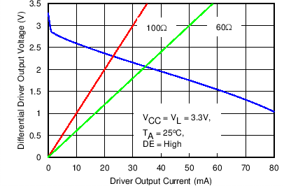
| |VOD| | Driver differential output voltage magnitude | RL = 60 Ω, 375 Ω on each output to –7 V to 12 V |
See Figure 9 | 1.5 | 2 | V | ||
| RL = 54 Ω (RS-485) | See Figure 10 | 1.5 | 2 | V | ||||
| RL = 100 Ω (RS-422) TJ ≥ 0°C, VCC ≥ 3.2V |
2 | V | ||||||
| Δ|VOD| | Change in magnitude of driver differential output voltage | RL = 54 Ω, CL = 50 pF | –50 | 0 | 50 | mV | ||
| VOC(SS) | Steady-state common-mode output voltage | Center of two 27-Ω load resistors | 1 | VCC/2 | 3 | V | ||
| ΔVOC | Change in differential driver output common-mode voltage | –50 | 0 | 50 | mV | |||
| VOC(PP) | Peak-to-peak driver common-mode output voltage | 500 | mV | |||||
| COD | Differential output capacitance | 15 | pF | |||||
| VIT+ | Positive-going receiver differential input voltage threshold | See (1) | –60 | –20 | mV | |||
| VIT– | Negative-going receiver differential input voltage threshold | –200 | –130 | See (1) | mV | |||
| VHYS | Receiver differential input voltage threshold hysteresis (VIT+ – VIT–) |
40 | 70 | mV | ||||
| VOH | Receiver high-level output voltage | VL = 1.65 V, IOH = -2 mA | 1.3 | 1.45 | V | |||
| VL = 3 V, IOH = -2 mA | 2.8 | 2.9 | ||||||
| VOL | Receiver low-level output voltage | VL = 1.65 V, IOL = 2 mA | 0.2 | 0.35 | V | |||
| VL = 3 V, IOL = 2 mA | 0.1 | 0.2 | ||||||
| II | Driver input, driver enable, and receiver enable input current | –2 | 2 | µA | ||||
| IOZ | Receiver output high-impedance current | VO = 0 V or VL, RE at VL | –1 | 1 | µA | |||
| IOS | Driver short-circuit output current | –150 | 150 | mA | ||||
| II | Bus input current (disabled driver) | VL = 1.8 V, VCC = 3.3 V, DE at 0 V |
VI = 12 V | 85 | 125 | µA | ||
| VI = –7 V | –100 | –60 | µA | |||||
| ICC | Supply current (quiescent) | Driver and Receiver enabled | DE=VL, RE = GND, No load | 750 | 1100 | µA | ||
| TJ ≤ 85°C | 1000 | µA | ||||||
| Driver enabled, receiver disabled | DE=VCC, RE = VL, No load | 350 | 650 | µA | ||||
| Driver disabled, receiver enabled | DE=GND, RE = GND, No load | 650 | 800 | µA | ||||
| Driver and receiver disabled | DE=GND, RE = VL, No load | 0.1 | 5 | µA | ||||
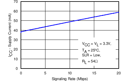
| Supply current (dynamic) | See the Typical Characteristics section | |||||||
(1) Under any specific conditions, VIT+ is specified to be at least VHYS higher than VIT–.
6.7 Switching Characteristics
over recommended operating conditions| PARAMETER | TEST CONDITIONS | MIN | TYP | MAX | UNIT | ||
|---|---|---|---|---|---|---|---|
| DRIVER, SLR = '1', 250 kbps, bit time ≥ 4 µs | |||||||
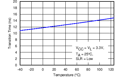
| tr, tf | Driver differential output rise/fall time | RL = 54 Ω, CL = 50 pF | See Figure 11 | 0.4 | 0.8 | 1.2 | µs |
| tPHL, tPLH | Driver propagation delay | 0.4 | 0.8 | 1.2 | µs | ||
| tSK(P) | Driver pulse skew, |tPHL – tPLH| | 0.2 | µs | ||||
| tPHZ, tPLZ | Driver disable time | See Figure 12 and Figure 13 | 0.025 | 0.1 | µs | ||
| tPZH, tPZL | Driver enable time | Receiver enabled | 0.6 | 1 | µs | ||
| Receiver disabled | 3.5 | 8 | µs | ||||
| DRIVER, SLR = '0', 20 Mbps, bit time ≥ 50 ns | |||||||
| tr, tf | Driver differential output rise/fall time | RL = 54 Ω, CL = 50 pF |
See Figure 11 | 5 | 10 | 15 | ns |
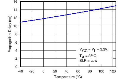
| tPHL, tPLH | Driver propagation delay | 6 | 15 | 25 | ns | ||
| tSK(P) | Driver pulse skew, |tPHL – tPLH| | 4 | ns | ||||
| tPHZ, tPLZ | Driver disable time | See Figure 12 and Figure 13 | 20 | 35 | ns | ||
| tPZH, tPZL | Driver enable time | Receiver enabled | 14 | 30 | ns | ||
| Receiver disabled | 3 | 7 | µs | ||||
| RECEIVER, SLR = 'X' | |||||||
| tr, tf | Receiver output rise/fall time | CL = 15 pF | See Figure 14 | 5 | 15 | ns | |
| tPHL, tPLH | Receiver propagation delay time | 30 | 60 | 90 | ns | ||
| tSK(P) | Receiver pulse skew, |tPHL – tPLH| | 15 | ns | ||||
| tPLZ, tPHZ | Receiver disable time | 10 | 20 | ns | |||
| tpZL(1), tPZH(1)
tPZL(2), tPZH(2) |
Receiver enable time | Driver enabled | See Figure 15 | 15 | 80 | ns | |
| Driver disabled | See Figure 16 | 3 | 8 | µs | |||
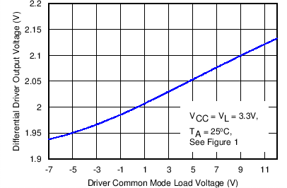
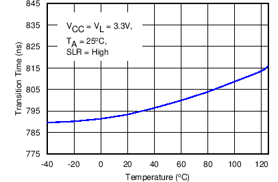
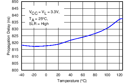
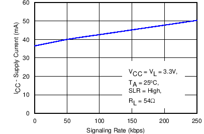
6.8 Typical Characteristics