ZHCSBS4F July   2013  – August 2014 SN65HVD01

PRODUCTION DATA.  

  1. 特性
  2. 应用范围
  3. 说明
  4. 修订历史记录
  5. Pin Configuration and Functions
  6. Specifications
    1. 6.1 Absolute Maximum Ratings
    2. 6.2 Handling Ratings
    3. 6.3 Recommended Operating Conditions
    4. 6.4 Thermal Information
    5. 6.5 Dissipation Ratings
    6. 6.6 Electrical Characteristics
    7. 6.7 Switching Characteristics
    8. 6.8 Typical Characteristics
  7. Parameter Measurement Information
  8. Detailed Description
    1. 8.1 Overview
    2. 8.2 Functional Block Diagram
    3. 8.3 Feature Description
    4. 8.4 Device Functional Modes
      1. 8.4.1 Equivalent Input and Output Schematic Diagrams
  9. Applications and Implementation
    1. 9.1 Application Information
    2. 9.2 Typical Application
      1. 9.2.1 Design Requirements
        1. 9.2.1.1 Data Rate and Bus Length
        2. 9.2.1.2 Bus Loading
      2. 9.2.2 Detailed Design Procedure
      3. 9.2.3 Application Performance Curves
  10. 10Power Supply Recommendations
  11. 11Layout
    1. 11.1 Layout Guidelines
    2. 11.2 Layout Example
  12. 12器件和文档支持
    1. 12.1 Trademarks
    2. 12.2 Electrostatic Discharge Caution
    3. 12.3 术语表
  13. 13机械封装和可订购信息

封装选项

机械数据 (封装 | 引脚)
散热焊盘机械数据 (封装 | 引脚)
订购信息

5 Pin Configuration and Functions

DRC 10 PIN
(TOP VIEW)
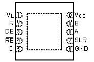
po_sllseh0.gif

Pin Functions

NAME NO. I/O DESCRIPTION
VL 1 Logic Supply 1.65 V to 3.6 V supply for logic I/O signals R, RE, D, DE, and SLR)
R 2 Digital Output Receive data output
DE 3 Digital Input Driver enable input
RE 4 Digital Input Receiver enable input
D 5 Digital Input Transmission data input
GND 6 Reference Potential Local device ground
SLR 7 Digital Input Slew rate select: Low = 20 Mbps, High = 250 kbps. Defaults to 20 Mbps if SLR is left floating
A 8 Bus I/O Digital bus I/O, A
B 9 Bus I/O Digital bus I/O, B
VCC 10 Bus Supply 3 V to 3.6 V supply for A and B bus lines