ZHCS075A June 2012 – September 2015 PCM2903C
PRODUCTION DATA.
- 1 特性
- 2 应用
- 3 说明
- 4 修订历史记录
- 5 Device Comparison Table
- 6 Pin Configuration and Functions
-
7 Specifications
- 7.1 Absolute Maximum Ratings
- 7.2 ESD Ratings
- 7.3 Recommended Operating Conditions
- 7.4 Thermal Information
- 7.5 Electrical Characteristics
- 7.6
Typical Characteristics
- 7.6.1 Typical Characteristics: ADC
- 7.6.2 Typical Characteristics: DAC
- 7.6.3 Typical Characteristics: ADC Output Spectrum
- 7.6.4 Typical Characteristics: DAC Output Spectrum
- 7.6.5 Typical Characteristics: Supply Current
- 7.6.6 Typical Characteristics: ADC Digital Decimation Filter Frequency Response
- 7.6.7 Typical Characteristics: ADC Digital High-Pass Filter Frequency Response
- 7.6.8 Typical Characteristics: ADC Analog Antialiasing Filter Frequency Response
- 7.6.9 Typical Characteristics: DAC Digital Interpolation Filter Frequency Response
- 7.6.10 Typical Characteristics: DAC Analog Fir Filter Frequency Response
- 7.6.11 Typical Characteristics: DAC Analog Low-Pass Filter Frequency Response
- 8 Parameter Measurement Information
- 9 Detailed Description
- 10Application and Implementation
- 11Power Supply Recommendations
- 12Layout
- 13器件和文档支持
- 14机械、封装和可订购信息
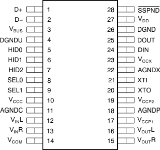
6 Pin Configuration and Functions
DB Package
28-Pin SSOP
Top View

Pin Functions
| PIN | I/O | DESCRIPTION | |
|---|---|---|---|
| NAME | NO. | ||
| AGNDC | 11 | – | Analog ground for codec |
| AGNDP | 18 | – | Analog ground for PLL |
| AGNDX | 22 | – | Analog ground for oscillator |
| D– | 2 | I/O | USB differential input/output minus(1) |
| D+ | 1 | I/O | USB differential input/output plus(1) |
| DGND | 26 | – | Digital ground |
| DGNDU | 4 | – | Digital ground for USB transceiver |
| DIN | 24 | I | S/PDIF input (2) |
| DOUT | 25 | O | S/PDIF output |
| HID0 | 5 | I | HID key state input (mute), active-high(3) |
| HID1 | 6 | I | HID key state input (volume up), active-high(3) |
| HID2 | 7 | I | HID key state input (volume down), active-high(3) |
| SEL0 | 8 | I | Must be set to high(4) |
| SEL1 | 9 | I | Connected to the USB port of VBUS(4) |
| SSPND | 28 | O | Suspend flag, active-low (Low: suspend, High: operational) |
| VBUS | 3 | – | Must be connected to VDD |
| VCCC | 10 | – | Analog power supply for codec(5) |
| VCCP1 | 17 | – | Analog power supply for PLL(5) |
| VCCP2 | 19 | – | Analog power supply for PLL(5) |
| VCCX | 23 | – | Analog power supply for oscillator(5) |
| VCOM | 14 | – | Common for ADC/DAC (VCCC/2) (5) |
| VDD | 27 | – | Digital power supply(5) |
| VINL | 12 | I | ADC analog input for L-channel |
| VINR | 13 | I | ADC analog input for R-channel |
| VOUTL | 16 | O | DAC analog output for L-channel |
| VOUTR | 15 | O | DAC analog output for R-channel |
| XTI | 21 | I | Crystal oscillator input(6) |
| XTO | 20 | O | Crystal oscillator output |
(1) LV-TTL level.
(2) 3.3-V CMOS-level input with internal pulldown, 5-V tolerant.
(3) 3.3-V CMOS-level input with internal pulldown. This pin informs the PC of serviceable control signals such as mute, volume up, or volume down, which have no direct connection with the internal DAC or ADC. See the Interface Number 3 and End-Points sections.
(4) TTL Schmitt trigger, 5-V tolerant.
(5) Connect a decoupling capacitor to GND.
(6) 3.3-V CMOS-level input.