ZHCSJO8 May   2019 OPA818

ADVANCE INFORMATION for pre-production products; subject to change without notice.  

  1. 特性
  2. 应用
    1.     高速光学前端
  3. 说明
    1.     光电二极管电容与 3dB 带宽间的关系
  4. 修订历史记录
  5. Pin Configuration and Functions
    1.     Pin Functions
  6. Specifications
    1. 6.1 Absolute Maximum Ratings
    2. 6.2 ESD Ratings
    3. 6.3 Recommended Operating Conditions
    4. 6.4 Thermal Information
    5. 6.5 Electrical Characteristics: VS = ±5 V
    6. 6.6 Typical Characteristics: VS = ±5 V
  7. Detailed Description
    1. 7.1 Overview
    2. 7.2 Functional Block Diagram
    3. 7.3 Feature Description
      1. 7.3.1 Input and ESD Protection
      2. 7.3.2 Feedback Pin
      3. 7.3.3 Decompensated Architecture With Wide Gain-Bandwidth Product
      4. 7.3.4 Low Input Capacitance
    4. 7.4 Device Functional Modes
      1. 7.4.1 Split-Supply Operation (+4/–2 V to ±6.5 V)
      2. 7.4.2 Single-Supply Operation (6 V to 13 V)
  8. Application and Implementation
    1. 8.1 Application Information
      1. 8.1.1 Wideband, Noninverting Operation
      2. 8.1.2 Wideband, Transimpedance Design Using OPA818
    2. 8.2 Typical Application
      1. 8.2.1 Design Requirements
      2. 8.2.2 Detailed Design Procedure
      3. 8.2.3 Application Curves
  9. Power Supply Recommendations
  10. 10Layout
    1. 10.1 Layout Guidelines
      1. 10.1.1 Thermal Considerations
    2. 10.2 Layout Example
  11. 11器件和文档支持
    1. 11.1 接收文档更新通知
    2. 11.2 社区资源
    3. 11.3 商标
    4. 11.4 静电放电警告
    5. 11.5 Glossary
  12. 12机械、封装和可订购信息
    1. 12.1 Package Option Addendum
      1. 12.1.1 Packaging Information

封装选项

机械数据 (封装 | 引脚)
散热焊盘机械数据 (封装 | 引脚)
订购信息

Pin Configuration and Functions

DRG Package
8-Pin WSON With Thermal Pad
Top View
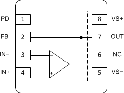
OPA818 SBOS940_OPA818_Pinout-DRG.gif
NC - no internal connection

Pin Functions

PIN TYPE DESCRIPTION
NAME WSON
FB 2 Output Feedback resistor connection (optional)
IN– 3 Input Inverting input
IN+ 4 Input Noninverting input
NC 6 No connect (no internal connection to die)
OUT 7 Output Output of amplifier
PD 1 Input Power down
VS– 5 Power Negative power supply
VS+ 8 Power Positive power supply
Thermal pad Electrically isolated from the die. Recommended connection to a heat spreading plane, typically GND.