ZHCSJO8 May   2019 OPA818

ADVANCE INFORMATION for pre-production products; subject to change without notice.  

  1. 特性
  2. 应用
    1.     高速光学前端
  3. 说明
    1.     光电二极管电容与 3dB 带宽间的关系
  4. 修订历史记录
  5. Pin Configuration and Functions
    1.     Pin Functions
  6. Specifications
    1. 6.1 Absolute Maximum Ratings
    2. 6.2 ESD Ratings
    3. 6.3 Recommended Operating Conditions
    4. 6.4 Thermal Information
    5. 6.5 Electrical Characteristics: VS = ±5 V
    6. 6.6 Typical Characteristics: VS = ±5 V
  7. Detailed Description
    1. 7.1 Overview
    2. 7.2 Functional Block Diagram
    3. 7.3 Feature Description
      1. 7.3.1 Input and ESD Protection
      2. 7.3.2 Feedback Pin
      3. 7.3.3 Decompensated Architecture With Wide Gain-Bandwidth Product
      4. 7.3.4 Low Input Capacitance
    4. 7.4 Device Functional Modes
      1. 7.4.1 Split-Supply Operation (+4/–2 V to ±6.5 V)
      2. 7.4.2 Single-Supply Operation (6 V to 13 V)
  8. Application and Implementation
    1. 8.1 Application Information
      1. 8.1.1 Wideband, Noninverting Operation
      2. 8.1.2 Wideband, Transimpedance Design Using OPA818
    2. 8.2 Typical Application
      1. 8.2.1 Design Requirements
      2. 8.2.2 Detailed Design Procedure
      3. 8.2.3 Application Curves
  9. Power Supply Recommendations
  10. 10Layout
    1. 10.1 Layout Guidelines
      1. 10.1.1 Thermal Considerations
    2. 10.2 Layout Example
  11. 11器件和文档支持
    1. 11.1 接收文档更新通知
    2. 11.2 社区资源
    3. 11.3 商标
    4. 11.4 静电放电警告
    5. 11.5 Glossary
  12. 12机械、封装和可订购信息
    1. 12.1 Package Option Addendum
      1. 12.1.1 Packaging Information

封装选项

机械数据 (封装 | 引脚)
散热焊盘机械数据 (封装 | 引脚)
订购信息

Feedback Pin

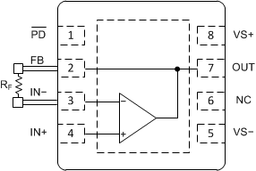
For high speed analog design, minimizing parasitic capacitances and inductances is critical to get the best performance from a high speed amplifier such as the OPA818. Parasitics are especially detrimental in the feedback path and at the inverting input. They result in undesired poles and zeroes in the feedback that could result in reduced phase margin or instability. Techniques used to correct for this phase margin reduction often result in reduced application bandwidth. To keep system engineers from making these tradeoff choices and to simplify the PCB layout, OPA818 features an FB pin on the same side as the inverting input pin, IN–. This allows for a very short feedback resistor, RF, connection between the FB and the IN– pin as shown in Figure 9, thus minimizing parasitics with minimal PCB design effort. Internally the FB pin is connected to VOUT via metal routing on the silicon. Due to the fixed metal sizing of this connection, FB pin has limited current carrying capability and specifications in the Absolute Maximum Ratings must be adhered to for continuous operation.
OPA818 SBOS940_OPA818_Pinout-DRG-Features.gifFigure 9. RF Connection Between FB and IN– Pins