ZHCSEI8C January 2016 – March 2018 OPA197 , OPA2197 , OPA4197
PRODUCTION DATA.
- 1 特性
- 2 应用
- 3 说明
- 4 修订历史记录
- 5 Pin Configuration and Functions
-
6 Specifications
- 6.1 Absolute Maximum Ratings
- 6.2 ESD Ratings
- 6.3 Recommended Operating Conditions
- 6.4 Thermal Information: OPA197
- 6.5 Thermal Information: OPA2197
- 6.6 Thermal Information: OPA4197
- 6.7 Electrical Characteristics: VS = ±4 V to ±18 V (VS = 8 V to 36 V)
- 6.8 Electrical Characteristics: VS = ±2.25 V to ±4 V (VS = 4.5 V to 8 V)
- 6.9 Typical Characteristics
- 7 Detailed Description
- 8 Application and Implementation
- 9 Power Supply Recommendations
- 10Layout
- 11器件和文档支持
- 12机械、封装和可订购信息
封装选项
机械数据 (封装 | 引脚)
散热焊盘机械数据 (封装 | 引脚)
- D|14
订购信息
8.2.3 Precision Reference Buffer
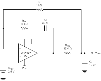
The OPAx197 features high output current drive capability and low input offset voltage, making the device an excellent reference buffer to provide an accurate buffered output with ample drive current for transients. For the 10-µF ceramic capacitor shown in Figure 56, RISO, a 37.4-Ω isolation resistor, provides separation of two feedback paths for optimal stability. Feedback path number one is through RF and is directly at the output, VOUT. Feedback path number two is through RFx and CF and is connected at the output of the op amp. The optimized stability components shown for the 10-µF load give a closed-loop signal bandwidth at VOUT of 4 kHz, while still providing a loop gain phase margin of 89°. Any other load capacitances require recalculation of the stability components: RF, RFx, CF, and RISO.
 Figure 56. Precision Reference Buffer