ZHCSEI8C January 2016 – March 2018 OPA197 , OPA2197 , OPA4197
PRODUCTION DATA.
- 1 特性
- 2 应用
- 3 说明
- 4 修订历史记录
- 5 Pin Configuration and Functions
-
6 Specifications
- 6.1 Absolute Maximum Ratings
- 6.2 ESD Ratings
- 6.3 Recommended Operating Conditions
- 6.4 Thermal Information: OPA197
- 6.5 Thermal Information: OPA2197
- 6.6 Thermal Information: OPA4197
- 6.7 Electrical Characteristics: VS = ±4 V to ±18 V (VS = 8 V to 36 V)
- 6.8 Electrical Characteristics: VS = ±2.25 V to ±4 V (VS = 4.5 V to 8 V)
- 6.9 Typical Characteristics
- 7 Detailed Description
- 8 Application and Implementation
- 9 Power Supply Recommendations
- 10Layout
- 11器件和文档支持
- 12机械、封装和可订购信息
封装选项
机械数据 (封装 | 引脚)
散热焊盘机械数据 (封装 | 引脚)
- D|14
订购信息
7.3.6 Common-Mode Voltage Range
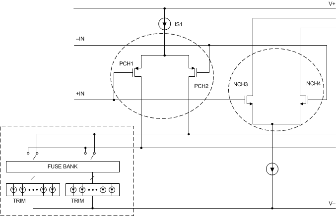
The OPAx197 is a 36-V, true rail-to-rail input operational amplifier with an input common-mode range that extends 100 mV beyond either supply rail. This wide range is achieved with paralleled complementary N-channel and P-channel differential input pairs, as shown in Figure 50. The N-channel pair is active for input voltages close to the positive rail, typically (V+) – 3 V to 100 mV above the positive supply. The P-channel pair is active for inputs from 100 mV below the negative supply to approximately (V+) – 1.5 V. There is a small transition region, typically (V+) –3 V to (V+) – 1.5 V in which both input pairs are on. This transition region can vary modestly with process variation, and within this region PSRR, CMRR, offset voltage, offset drift, noise and THD performance may be degraded compared to operation outside this region.
 Figure 50. Rail-to-Rail Input Stage
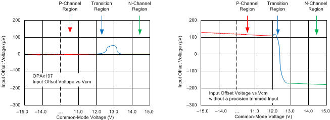
To achieve the best performance for two-stage rail-to-rail input amplifiers, avoid the transition region when possible. The OPAx197 uses a precision trim for both the N-channel and P-channel regions. This technique enables significantly lower levels of offset than previous-generation devices, causing variance in the transition region of the input stages to appear exaggerated relative to offset over the full common-mode voltage range, as shown in Figure 51.
 Figure 51. Common-Mode Transition vs Standard Rail-to-Rail Amplifiers