ZHCSEI8C January 2016 – March 2018 OPA197 , OPA2197 , OPA4197
PRODUCTION DATA.
- 1 特性
- 2 应用
- 3 说明
- 4 修订历史记录
- 5 Pin Configuration and Functions
-
6 Specifications
- 6.1 Absolute Maximum Ratings
- 6.2 ESD Ratings
- 6.3 Recommended Operating Conditions
- 6.4 Thermal Information: OPA197
- 6.5 Thermal Information: OPA2197
- 6.6 Thermal Information: OPA4197
- 6.7 Electrical Characteristics: VS = ±4 V to ±18 V (VS = 8 V to 36 V)
- 6.8 Electrical Characteristics: VS = ±2.25 V to ±4 V (VS = 4.5 V to 8 V)
- 6.9 Typical Characteristics
- 7 Detailed Description
- 8 Application and Implementation
- 9 Power Supply Recommendations
- 10Layout
- 11器件和文档支持
- 12机械、封装和可订购信息
封装选项
机械数据 (封装 | 引脚)
散热焊盘机械数据 (封装 | 引脚)
- D|14
订购信息
7.3.5 Capacitive Load and Stability
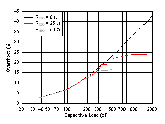
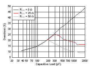
The OPAx197 features a patented output stage capable of driving large capacitive loads, and in a unity-gain configuration, directly drives up to 1 nF of pure capacitive load. Increasing the gain enhances the ability of the amplifier to drive greater capacitive loads; see Figure 47 and Figure 48. The particular op amp circuit configuration, layout, gain, and output loading are some of the factors to consider when establishing whether an amplifier will be stable in operation.
 Figure 47. Small-Signal Overshoot vs Capacitive Load (100-mV Output Step, G = –1 V/V)
 Figure 48. Small-Signal Overshoot vs Capacitive Load (100-mV Output Step, G = 1 V/V)
For additional drive capability in unity-gain configurations, improve capacitive load drive by inserting a small
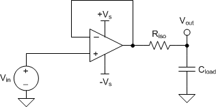
(10-Ω to 20-Ω) resistor, RISO, in series with the output, as shown in Figure 49. This resistor significantly reduces ringing while maintaining dc performance for purely capacitive loads. However, if there is a resistive load in parallel with the capacitive load, a voltage divider is created, introducing a gain error at the output and slightly reducing the output swing. The error introduced is proportional to the ratio RISO / RL, and is generally negligible at low output levels. A high capacitive load drive makes the OPA197 well suited for applications such as reference buffers, MOSFET gate drives, and cable-shield drives. The circuit shown in Figure 49 uses an isolation resistor, RISO, to stabilize the output of an op amp. RISO modifies the open-loop gain of the system for increased phase margin, and results using the OPA197 are summarized in Table 3. For additional information on techniques to optimize and design using this circuit, TI Precision Design TIDU032 details complete design goals, simulation, and test results.
 Figure 49. Extending Capacitive Load Drive with the OPA197
Table 3. OPA197 Capacitive Load Drive Solution Using Isolation Resistor Comparison of Calculated and Measured Results
| PARAMETER | VALUE | |||||||||
|---|---|---|---|---|---|---|---|---|---|---|
| Capacitive Load | 100 pF | 1000 pF | 0.01 µF | 0.1 µF | 1 µF | |||||
| Phase Margin | 45° | 60° | 45° | 60° | 45° | 60° | 45° | 60° | 45° | 60° |
| RISO (Ω) | 47.0 | 360.0 | 24.0 | 100.0 | 20.0 | 51.0 | 6.2 | 15.8 | 2.0 | 4.7 |
| Measured Overshoot (%) | 23.2 8.6 | 10.4 | 22.5 | 9.0 | 22.1 | 8.7 | 23.1 | 8.6 | 21.0 | 8.6 |
| Calculated PM | 45.1° | 58.1° | 45.8° | 59.7° | 46.1° | 60.1° | 45.2° | 60.2° | 47.2° | 60.2° |

|
For step-by-step design procedure, circuit schematics, bill of materials, printed circuit board (PCB) files, simulation results, and test results, refer to TI Precision Design TIDU032, Capacitive Load Drive Solution using an Isolation Resistor . |