ZHCSIQ3B September 2018 – June 2019 OPA2156
PRODUCTION DATA.
- 1 特性
- 2 应用
- 3 说明
- 4 修订历史记录
- 5 Pin Configuration and Functions
- 6 Specifications
- 7 Detailed Description
- 8 Application and Implementation
- 9 Power Supply Recommendations
- 10Layout
- 11器件和文档支持
- 12机械、封装和可订购信息
封装选项
机械数据 (封装 | 引脚)
散热焊盘机械数据 (封装 | 引脚)
- DGK|8
订购信息
8.2.2 Detailed Design Procedure
In this example the OPA2156 serves as a transimpedance amplifier for a differential photodiode. The differential configuration allows for a wider output range (0 to 10-V differential) compared to a single-ended configuration (0 V to 5 V). This output can be connected to a differential successive approximation register (SAR) analog-to-digital converter (ADC). The basic equation for a differential transimpedance amplifier output voltage is shown in Equation 3.

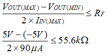
Equation 3 can be rearranged to calculate the value of the feedback resistors as shown in Equation 4.

Adding a capacitor to the feedback loop creates a filter which will remove undesired noise beyond its cutoff frequency. For this application a 1-MHz cutoff frequency was selected. The equation for an RC filter is provided in Equation 5.

Rearranging this equation to solve for the capacitor value is show in Equation 6.

For more information on photodiode transimpedance amplifier system design and for a single-ended example, see TIDU535: 1 MHz, Single-Supply, Photodiode Amplifier Reference Design.