SNVSA15B December   2013  – December 2015 LP8557

PRODUCTION DATA.  

  1. Features
  2. Applications
  3. Description
  4. Revision History
  5. Device Comparison Table
  6. Pin Function and Configurations
  7. Specifications
    1. 7.1  Absolute Maximum Ratings
    2. 7.2  ESD Ratings
    3. 7.3  Recommended Operating Conditions
    4. 7.4  Thermal Information
    5. 7.5  Electrical Characteristics
    6. 7.6  Boost Converter Electrical Characteristics
    7. 7.7  LED Driver Electrical Characteristics (LED1 To LED6 Pins)
    8. 7.8  PWM Interface Characteristics (PWM Pin)
    9. 7.9  Logic Interface Characteristics (PWM, FSET/SDA, ISET/SCL Pins)
    10. 7.10 I2C Serial Bus Timing Parameters (SDA, SCL)
    11. 7.11 Typical Characteristics
  8. Detailed Description
    1. 8.1 Overview
    2. 8.2 Functional Block Diagram
    3. 8.3 Feature Description
      1. 8.3.1 Boost Converter Overview
        1. 8.3.1.1 Operation
        2. 8.3.1.2 Adaptive Boost Output Voltage Control
      2. 8.3.2 Brightness Control
        1. 8.3.2.1 PWM Input Duty Measurement
        2. 8.3.2.2 BRTMODE = 00b
        3. 8.3.2.3 BRTMODE = 01b
        4. 8.3.2.4 BRTMODE = 10b
        5. 8.3.2.5 BRTMODE = 11b
        6. 8.3.2.6 Hybrid PWM & I Dimming Control
        7. 8.3.2.7 Phase Shift PWM Scheme
      3. 8.3.3 Slope and Advanced Slope
      4. 8.3.4 LED String Count Auto Detection
      5. 8.3.5 EMI Reduction Schemes
      6. 8.3.6 Fault Detection
        1. 8.3.6.1 LED Short Detection
        2. 8.3.6.2 LED OPEN* Detection
        3. 8.3.6.3 Undervoltage Detection
        4. 8.3.6.4 Thermal Shutdown
        5. 8.3.6.5 Boost Overcurrent Protection
        6. 8.3.6.6 Boost Overvoltage Protection
        7. 8.3.6.7 Boost Undervoltage Protection
    4. 8.4 Device Functional Modes
      1. 8.4.1 Shutdown Mode
      2. 8.4.2 Active Mode
    5. 8.5 Programming
      1. 8.5.1 I2C-Compatible Serial Bus Interface
        1. 8.5.1.1 Interface Bus Overview
        2. 8.5.1.2 Start and Stop Conditions
        3. 8.5.1.3 Data Transactions
        4. 8.5.1.4 Acknowledge Cycle
        5. 8.5.1.5 Acknowledge After Every Byte Rule
        6. 8.5.1.6 Control Register Write Cycle
        7. 8.5.1.7 Control Register Read Cycle
        8. 8.5.1.8 Register Read and Write Detail
    6. 8.6 Register Maps
      1. 8.6.1 Register Bit Descriptions
        1. 8.6.1.1  COMMAND
        2. 8.6.1.2  STATUS
        3. 8.6.1.3  BRTLO
        4. 8.6.1.4  BRTHI
        5. 8.6.1.5  CONFIG
        6. 8.6.1.6  CURRENT
        7. 8.6.1.7  PGEN
        8. 8.6.1.8  BOOST
        9. 8.6.1.9  LEDEN
        10. 8.6.1.10 STEP
  9. Application and Implementation
    1. 9.1 Application Information
      1. 9.1.1 Designing With LP8557
        1. 9.1.1.1 Setting Boost Switching and PWM Dimming Frequencies
        2. 9.1.1.2 Setting Boost Compensation
        3. 9.1.1.3 Setting Full-Scale Led Current
      2. 9.1.2 Designing With LP8557I
        1. 9.1.2.1 Setting Boost Switching Frequency
        2. 9.1.2.2 Setting Boost Compensation
        3. 9.1.2.3 Setting PWM Dimming Frequency
        4. 9.1.2.4 Setting Full-Scale LED Current
    2. 9.2 Typical Applications
      1. 9.2.1 LP8557 PWM-Only Option
        1. 9.2.1.1 Design Requirements
        2. 9.2.1.2 Detailed Design Procedure
          1. 9.2.1.2.1 Boost Output Capacitor Selection
          2. 9.2.1.2.2 Schottky Diode Selection
          3. 9.2.1.2.3 Inductor Selection
          4. 9.2.1.2.4 Boost Input andVDD Capacitor Selection
        3. 9.2.1.3 Application Curves
      2. 9.2.2 LP8557I PWM and I2C Device Option
        1. 9.2.2.1 Design Requirements
        2. 9.2.2.2 Detailed Design Procedure
        3. 9.2.2.3 Application Curves
  10. 10Power Supply Recommendations
  11. 11Layout
    1. 11.1 Layout Guidelines
      1. 11.1.1 Boost Output Capacitor Placement
      2. 11.1.2 Schottky Diode Placement
      3. 11.1.3 Inductor Placement
      4. 11.1.4 Boost Input and VDD Capacitor Placement
    2. 11.2 Layout Example
  12. 12Device and Documentation Support
    1. 12.1 Device Support
      1. 12.1.1 Third-Party Products Disclaimer
    2. 12.2 Related Links
    3. 12.3 Community Resources
    4. 12.4 Trademarks
    5. 12.5 Electrostatic Discharge Caution
    6. 12.6 Glossary
  13. 13Mechanical, Packaging, and Orderable Information

封装选项

机械数据 (封装 | 引脚)
散热焊盘机械数据 (封装 | 引脚)
订购信息

6 Pin Function and Configurations

YFQ Package
16-Pin DSBGA
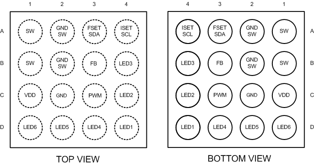
LP8557 LP85571 30162677.gif

Pin Functions

PIN TYPE (1) DESCRIPTION
NAME NO.
FB B3 A Boost feedback pin. The FB and OVP circuitry monitors the voltage on this pin.
FSET/SDA A3 I/O Dual function pin. When I2C is not used (for example, BRTMODE = 00b), this pin can be used to set ƒSW and/or ƒPWM by connecting a resistor from this pin to a ground reference. When I2C is used (for example, BRTMODE = 01, 10 or 11), connect this pin to an SDA line of an I2C bus. The LP8557 "PWM Only" device option uses this pin as an FSET pin. LP8557I "PWM and I2C" device option uses this pin as an SDA pin.
GND C2 G Ground pin.
ISET/SCL A4 I Dual function pin. When I2C is not used (for example, BRTMODE = 00b), this pin can be used to set the full-scale LED current by connecting a resistor from the pin to a ground reference. When I2C is used (for example, BRTMODE =01, 10, or 11), connect this pin to an SCL line of an I2C bus. The LP8557 "PWM Only" device option uses this pin as an ISET pin. LP8557I "PWM and I2C" device option uses this pin as an SCL pin.
LED1 D4 A LED driver – current sink terminal. If unused, this pin may be left floating.
LED2 C4 A LED driver – current sink terminal. If unused, this pin may be left floating.
LED3 B4 A LED driver – current sink terminal. If unused, this pin may be left floating.
LED4 D3 A LED driver – current sink terminal. If unused, this pin may be left floating.
LED5 D2 A LED driver – current sink terminal. If unused, this pin may be left floating.
LED6 D1 A LED driver – current sink terminal. If unused, this pin may be left floating.
PWM C3 I PWM input pin.
SW A1, B1 A A connection to the drain terminal of the integrated power MOSFET.
SW_GND A2, B2 G A connection to the source terminal of the integrated power MOSFET.
VDD C1 P Device power supply pin.
(1) A: Analog Pin, G: Ground Pin, P: Power Pin, I: Digital Input Pin, I/O: Digital Input/Output Pin