SNVSA15B December 2013 – December 2015 LP8557
PRODUCTION DATA.
- 1 Features
- 2 Applications
- 3 Description
- 4 Revision History
- 5 Device Comparison Table
- 6 Pin Function and Configurations
-
7 Specifications
- 7.1 Absolute Maximum Ratings
- 7.2 ESD Ratings
- 7.3 Recommended Operating Conditions
- 7.4 Thermal Information
- 7.5 Electrical Characteristics
- 7.6 Boost Converter Electrical Characteristics
- 7.7 LED Driver Electrical Characteristics (LED1 To LED6 Pins)
- 7.8 PWM Interface Characteristics (PWM Pin)
- 7.9 Logic Interface Characteristics (PWM, FSET/SDA, ISET/SCL Pins)
- 7.10 I2C Serial Bus Timing Parameters (SDA, SCL)
- 7.11 Typical Characteristics
-
8 Detailed Description
- 8.1 Overview
- 8.2 Functional Block Diagram
- 8.3 Feature Description
- 8.4 Device Functional Modes
- 8.5 Programming
- 8.6 Register Maps
- 9 Application and Implementation
- 10Power Supply Recommendations
- 11Layout
- 12Device and Documentation Support
- 13Mechanical, Packaging, and Orderable Information
9 Application and Implementation
NOTE
Information in the following applications sections is not part of the TI component specification, and TI does not warrant its accuracy or completeness. TI’s customers are responsible for determining suitability of components for their purposes. Customers should validate and test their design implementation to confirm system functionality.
9.1 Application Information
9.1.1 Designing With LP8557
The LP8557 is intended for applications without an I2C master. It can be fully controlled with an external PWM signal. Boost switching frequency, boost compensation, PWM dimming frequency, and the maximum LED current can be set with external resistors.
9.1.1.1 Setting Boost Switching and PWM Dimming Frequencies
Boost switching frequency and PWM dimming frequency are set by connecting a resistor from the FSET pin to GND. Available options are shown in Table 2.
Table 2. Setting Boost Switching and PWM Dimming Frequencies With an External Resistor
| RFSET [Ω] (TOLERANCE) | ƒSW (kHz) | ƒPWM (kHz) |
|---|---|---|
| 470k - 1M (±5%) | 500 | 4.9 |
| 300k, 330k (±5%) | 500 | 9.8 |
| 200k (±5%) | 500 | 14.6 |
| 147k, 150k, 154k, 158k (±1%) | 500 | 19.5 |
| 121k (±1%) | 500 | 24.4 |
| 100k (±1%) | 500 | 29.3 |
| 86.6k (±1%) | 500 | 34.2 |
| 75.0k (±1%) | 500 | 39.1 |
| 63.4k (±1%) | 1000 | 4.9 |
| 52.3k, 53.6k (±1%) | 1000 | 9.8 |
| 44.2k, 45.3k (±1%) | 1000 | 14.6 |
| 39.2k (±1%) | 1000 | 19.5 |
| 34.0k (±1%) | 1000 | 24.4 |
| 30.1k (±1%) | 1000 | 29.3 |
| 26.1k (±1%) | 1000 | 34.2 |
| 23.2k (±1%) | 1000 | 39.1 |
| 0 (grounded) | 500 | 9.8 |
9.1.1.2 Setting Boost Compensation
For stable LP8557 boost operation, appropriate boost compensation must be selected based on the selected boost switching frequency and the boost inductance. Table 3 shows recommended boost compensation options based on the boost switching frequency and selected boost circuit inductance.
Table 3. Recommended Boost Compensation Options Based
on the Boost Switching Frequency and Inductance
| ƒSW (kHz) | L (µH) | RECOMMENDED BOOST COMPENSATION OPTION |
|---|---|---|
| 500 | 10 15 22 |
1 1 0 |
| 1000 | 4.7 6.8 10 |
1 1 0 |
The LP8557 boost converter compensation is set by placing an external resistor, RISET, from the ISET pin to GND. Note that the ISET pin is shared for setting the full-scale LED current in addition to setting the boost compensation. Setting the boost compensation and the full-scale LED current using an external resistor is shown in Table 4.
9.1.1.3 Setting Full-Scale Led Current
The LP8557 full-scale current is set by placing an external resistor, RISET, from the ISET pin to GND. Note that the ISET pin is shared for setting the boost compensation in addition to the full-scale LED current. Setting the boost compensation and the full-scale LED current using an external resistor is shown in Table 4.
Table 4. Setting Full-Scale LED Current and Boost Compensation Using an External Resistor
| RISET [Ω] (TOLERANCE) | BOOST COMPENSATION OPTION | ILED (mA) |
|---|---|---|
| 470k - 1M (±5%) | 1 | 5 |
| 300k, 330k (±5%) | 1 | 10 |
| 200k (±5%) | 1 | 13 |
| 147k, 150k, 154k, 158k (±1%) | 1 | 15 |
| 121k (±1%) | 1 | 18 |
| 100k (±1%) | 1 | 20 |
| 86.6k (±1%) | 1 | 23 |
| 75.0k (±1%) | 1 | 25 |
| 63.4k (±1%) | 0 | 5 |
| 52.3k, 53.6k (±1%) | 0 | 10 |
| 44.2k, 45.3k (±1%) | 0 | 13 |
| 39.2k (±1%) | 0 | 15 |
| 34.0k (±1%) | 0 | 18 |
| 30.1k (±1%) | 0 | 20 |
| 26.1k (±1%) | 0 | 23 |
| 23.2k (±1%) | 0 | 25 |
| 0 (grounded) | 1 | 20 |
9.1.2 Designing With LP8557I
The LP8557I is intended for applications that can utilize an I2C master to control the device. Use of an external PWM signal is allowed for controlling the brightness levels; however, I2C commands are required to turn the backlight on or off. Boost switching frequency, boost compensation, PWM dimming frequency, and the maximum LED current are set to default values. Re-configuration is possible with I2C writes; however, re-programming has to be done every time power on the VDD pin is recycled.
9.1.2.1 Setting Boost Switching Frequency
The LP8557I boost converter switching frequency is set to 500 kHz by default. It may be re-programmed by overriding the BFREQ bit with an I2C write. Table 5 shows the boost switching frequency options available.
Table 5. Available Boost Switching Frequencies
| BFREQ | ƒSW [kHz] |
|---|---|
| 0 | 500 |
| 1 | 1000 |
9.1.2.2 Setting Boost Compensation
For stable LP8557I boost operation, appropriate boost compensation must be selected based on the selected boost switching frequency and the boost inductance. Table 6 shows recommended boost compensation options based on the boost switching frequency and selected boost circuit inductance.
Table 6. Recommended Boost Compensation Options Based
on the Boost Switching Frequency and Inductance
| ƒSW (kHz) | L (µH) | RECOMMENDED BOOST COMPENSATION OPTION |
|---|---|---|
| 500 | 10 15 22 |
1 1 0 |
| 1000 | 4.7 6.8 10 |
1 1 0 |
The LP8557I boost converter compensation is set to option 1 by default. It may be re-programmed by overriding the BCOMP bit with an I2C write. Table 7 shows available boost compensation options.
Table 7. Available Boost Compensation Options
| BCOMP | BOOST COMPENSATION OPTION |
|---|---|
| 0 | 0 |
| 1 | 1 |
9.1.2.3 Setting PWM Dimming Frequency
The LP8557I PWM dimming frequency is set to 9.8 kHz by default. It may be re-programmed by overriding the PFREQ bits with an I2C write. Table 8 summarizes available PWM dimming frequencies.
Table 8. Available PWM Dimming Frequencies
| PFREQ | ƒPWM (kHz) |
|---|---|
| 000 | 4.9 |
| 001 | 9.8 |
| 010 | 14.6 |
| 011 | 19.5 |
| 100 | 24.4 |
| 101 | 29.3 |
| 110 | 34.2 |
| 111 | 39.1 |
9.1.2.4 Setting Full-Scale LED Current
The LP8557I full-scale LED current is set to 25 mA by default. It may be re-programmed by overriding MAXCURR bits with an I2C write. Table 9 shows available full-scale LED current levels.
Table 9. Available Full-Scale LED Currents
| MAXCURR | ILED [mA] |
|---|---|
| 000 | 5 |
| 001 | 10 |
| 010 | 13 |
| 011 | 15 |
| 100 | 18 |
| 101 | 20 |
| 110 | 23 |
| 111 | 25 |
9.2 Typical Applications
9.2.1 LP8557 PWM-Only Option
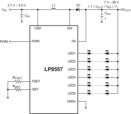 Figure 38. LP8557 PWM-Only Device Option
9.2.1.1 Design Requirements
Table 10. Recommended Inductance
| MIN | TYP | MAX | UNIT | |
|---|---|---|---|---|
| ƒsw = 1 MHz | 3.29 | 4.7 - 10 | µH | |
| ƒsw = 500 kHz | 7 | 10 - 22 |
Table 11. Recommended Output Capacitance(1)
| MIN | TYP | MAX | UNIT | |
|---|---|---|---|---|
| ƒsw = 1 MHz | 2 | µF | ||
| ƒsw = 500 kHz | 2 |
9.2.1.2 Detailed Design Procedure
9.2.1.2.1 Boost Output Capacitor Selection
The LP8557 inductive boost converter typically requires two 4.7-µF output capacitors. The voltage rating of the capacitor must be 35 V or higher as the OVP threshold is at 29.6 V (typ). Pay careful attention to the capacitor tolerance and DC bias response. For proper operation the degradation in capacitance due to tolerance, DC bias, and temperature should stay above 2 µF. This might require placing more than two devices in parallel in order to maintain the required output capacitance over the device operating temperature and output voltage range.
9.2.1.2.2 Schottky Diode Selection
The Schottky diode must have a reverse breakdown voltage greater than the LP8557’s maximum output voltage. Additionally, the diode must have an average current rating high enough to handle the LP8557 maximum output current; at the same time the diode's peak current rating must be high enough to handle the peak inductor current. Schottky diodes are required due to their lower forward voltage drop (0.3V to 0.5V) and their fast recovery time.
9.2.1.2.3 Inductor Selection
The chosen inductor must be from 10 to 22 µH (for 500-kHz operation) or 4.7 to 10 µH (for 1-MHz operation) and must have a saturation rating equal to, or greater than, the circuit's peak operating current. IPEAK can be found by the following calculation:

This assumes the device is operating in continuous conduction mode (CCM) which is typically the case when operating near the peak current. For smaller rated inductors, and when the device is operating in discontinuous conduction mode (DCM), the peak current can be found from:

The device operates in CCM when the following is true:

9.2.1.2.4 Boost Input andVDD Capacitor Selection
The LP8557 VDD pin is typically tied to the same supply as the input of the boost power stage (VIN node). A 10-µF input capacitor is recommended on that node. The voltage rating of the capacitor must be at least 10 V. If a supply powering the VDD pin is different from a supply powering the boost power stage, then 10-µF input capacitors are required on both VDD and VIN nodes.
9.2.1.3 Application Curves
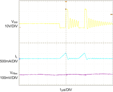 Figure 39. Steady State Operation With Light Load
 (200 µA/String, 6 Strings)
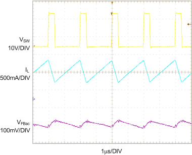 Figure 41. Steady State Operation With Heavy Load
 (25 mA/String, 6 Strings)
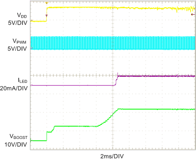 Figure 43. Start-Up With a 50% Input PWM Duty
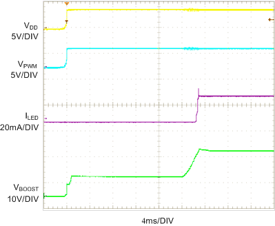 Figure 45. Start-Up With a 100% Input PWM Duty
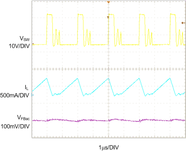 Figure 40. Steady State Operation With Medium Load
 (5 mA/String, 6 Strings)
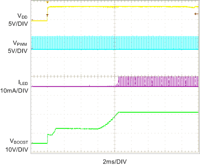 Figure 42. Start-Up With a 1% Input PWM Duty
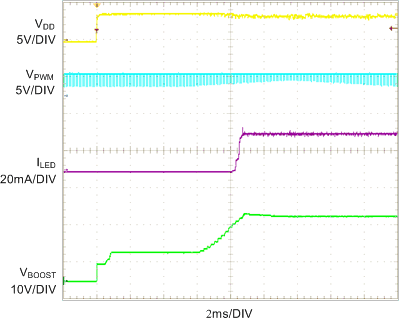 Figure 44. Start-Up With a 99% Input PWM Duty
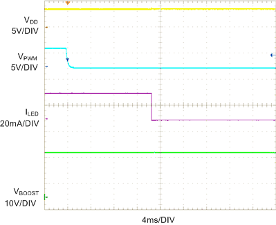 Figure 46. Shutdown Operation
9.2.2 LP8557I PWM and I2C Device Option
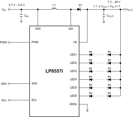 Figure 47. Typical Application With LP8557I PWM and I2C Device Option
9.2.2.1 Design Requirements
See Design Requirements.
9.2.2.2 Detailed Design Procedure
9.2.2.3 Application Curves
See Application Curves.