ZHCSD18A March 2013 – October 2014 LP55231
PRODUCTION DATA.
- 1 特性
- 2 应用
- 3 说明
- 4 修订历史记录
- 5 Pin Configuration and Functions
-
6 Specifications
- 6.1 Absolute Maximum Ratings
- 6.2 Handling Ratings
- 6.3 Recommended Operating Conditions
- 6.4 Thermal Information
- 6.5 Electrical Characteristics
- 6.6 Charge Pump Electrical Characteristics
- 6.7 LED Driver Electrical Characteristics
- 6.8 LED Test Electrical Characteristics
- 6.9 Logic Interface Characteristics
- 6.10 Recommended External Clock Source Conditions
- 6.11 Serial Bus Timing Parameters (SDA, SCL)
- 6.12 Typical Characteristics
-
7 Detailed Description
- 7.1 Overview
- 7.2 Functional Block Diagram
- 7.3 Feature Description
- 7.4 Device Functional Modes
- 7.5 Programming
- 7.6 Register Maps
- 8 Application and Implementation
- 9 Power Supply Recommendations
- 10Layout
- 11器件和文档支持
- 12机械封装和可订购信息
6 Specifications
6.1 Absolute Maximum Ratings
over operating free-air temperature range (unless otherwise noted) (1)(2)| MIN | MAX | UNIT | ||
|---|---|---|---|---|
| Voltage | Voltage on power pin VDD | −0.3 | 6 | V |
| Voltage on D1 to D9, C1−, C1+, C2−, C2+, VOUT |
−0.3 V to VDD +0.3V with 6 V max | V | ||
| Power | Continuous power dissipation(3) | Internally limited | ||
| Temperature | Junction temperature (TJ-MAX) | 125 | °C | |
| Maximum lead temperature (soldering) | See (4) | |||
(1) Stresses beyond those listed under Absolute Maximum Ratings may cause permanent damage to the device. These are stress ratings only, which do not imply functional operation of the device at these or any other conditions beyond those indicated under Recommended Operating Conditions. Exposure to absolute-maximum-rated conditions for extended periods may affect device reliability.
(2) All voltage are with respect to the potential at the GND pin.
(3) Internal thermal shutdown circuitry protects the device from permanent damage. Thermal shutdown engages at TJ = 150°C (typ.) and disengages at TJ = 130°C (typ.).
(4) For detailed soldering specifications and information, please refer to Texas Instruments Application Note AN-1187: Leadless Leadframe Package (LLP)(SNOA401).
6.2 Handling Ratings
| MIN | MAX | UNIT | |||
|---|---|---|---|---|---|
| Tstg | Storage temperature range | –65 | 150 | °C | |
| V(ESD) | Electrostatic discharge | Human body model (HBM), per ANSI/ESDA/JEDEC JS-001, all pins(1) | –2500 | 2500 | V |
| Charged device model (CDM), per JEDEC specification JESD22-C101, all pins(2) | –1000 | 1000 | |||
| Machine model: all pins | –250 | 250 | |||
(1) JEDEC document JEP155 states that 500-V HBM allows safe manufacturing with a standard ESD control process.
(2) JEDEC document JEP157 states that 250-V CDM allows safe manufacturing with a standard ESD control process.
6.3 Recommended Operating Conditions(1)(2)
Over operating free-air temperature range (unless otherwise noted)| MIN | NOM | MAX | UNIT | ||
|---|---|---|---|---|---|
| VDD | Input voltage | 2.7 | 5.5 | V | |
| Voltage on logic pins (input or output pins) | 0 | VDD | |||
| IOUT | Recommended charge pump load current | 0 | 100 | mA | |
| TJ | Junction temperature | −30 | 125 | °C | |
| TA | Ambient temperature(3) | −30 | 85 | ||
(1) Stresses beyond those listed under Absolute Maximum Ratings may cause permanent damage to the device. These are stress ratings only, which do not imply functional operation of the device at these or any other conditions beyond those indicated under Recommended Operating Conditions. Exposure to absolute-maximum-rated conditions for extended periods may affect device reliability.
(2) All voltage are with respect to the potential at the GND pin.
(3) In applications where high power dissipation and/or poor package thermal resistance is present, the maximum ambient temperature may have to be derated. Maximum ambient temperature (TA-MAX) is dependent on the maximum operating junction temperature (TJ-MAX-OP = 125°C), the maximum power dissipation of the device in the application (PD-MAX), and the junction-to ambient thermal resistance of the part/package in the application (θJA), as given by the following equation: TA-MAX = TJ-MAX-OP – (RθJA × PD-MAX).
6.4 Thermal Information
| THERMAL METRIC(1) | LP55231 | UNIT | |
|---|---|---|---|
| WQFN (RTW) | |||
| 24 PINS | |||
| RθJA | Junction-to-ambient thermal resistance(2) | 36.6 | °C/W |
(1) For more information about traditional and new thermal metrics, see the IC Package Thermal Metrics application report, SPRA953.
(2) Junction-to-ambient thermal resistance is highly application and board-layout dependent. In applications where high maximum power dissipation exists, special care must be paid to thermal dissipation issues in board design.
6.5 Electrical Characteristics(1)(2)(3)
Typical (TYP) values apply for TA = 25°C and minimum (MIN) and maximum (MAX) apply over the operating ambient temperature range (−30°C < TA < 85°C). Specifications apply to the LP55231 Functional Block Diagram with: VDD = 3.6 V, VEN = 1.65 V, COUT = 1 µF, CIN = 1 µF, C1–2 = 0.47 µF, unless otherwise specified.(4)| PARAMETER | TEST CONDITIONS | MIN | TYP | MAX | UNIT | |
|---|---|---|---|---|---|---|
| IVDD | Standby supply current | VEN = 0V, CHIP_EN=0 (bit), external 32-kHz clock running or not running | 0.2 | 1 | µA | |
| CHIP_EN=0 (bit), external 32-kHz clock not running | 1 | 1.7 | µA | |||
| CHIP_EN=0 (bit), external 32-kHz clock running | 1.4 | 2.3 | µA | |||
| Normal mode supply current | External 32-kHz clock running, charge pump and current source outputs disabled | 0.6 | 0.75 | mA | ||
| Charge pump in 1x mode, no load, current source outputs disabled | 0.8 | 0.95 | mA | |||
| Charge pump in 1.5x mode, no load, current source outputs disabled | 1.8 | mA | ||||
| Power save mode supply current | External 32-kHz clock running | 10 | 15 | µA | ||
| Internal oscillator running | 0.6 | 0.75 | mA | |||
| ƒOSC | Internal oscillator frequency accuracy | TA = 25°C | −4% | 4% | ||
| –7% | 7% | |||||
(1) The Electrical Characteristics tables list specifications under the listed Recommended Operating Conditions except as otherwise modified or specified by the Electrical Characteristics Test Conditions and/or Notes. Typical specifications are estimations only and are not verified.
(2) All voltages are with respect to the potential at the GND pin.
(3) Min and Max limits are verified by design, test, or statistical analysis.
(4) Low-ESR Surface-Mount Ceramic Capacitors (MLCCs) used in setting electrical characteristics.
6.6 Charge Pump Electrical Characteristics
Typical (TYP) values apply for TA = 25°C and minimum (MIN) and maximum (MAX) apply over the operating ambient temperature range (−30°C < TA < 85°C). Specifications apply to the LP55231 Functional Block Diagram with: VDD = 3.6 V, VEN = 1.65 V, COUT = 1 µF, CIN = 1 µF, C1–2 = 0.47 µF, unless otherwise specified.(1)| PARAMETER | TEST CONDITIONS | MIN | TYP | MAX | UNIT | |
|---|---|---|---|---|---|---|
| ROUT | Charge pump output resistance | Gain = 1.5x Gain = 1x |
3.5 1 |
Ω | ||
| ƒSW | Switching frequency | 1.25 | MHz | |||
| IGND | Ground current | Gain = 1.5x Gain = 1x |
1.2 0.3 |
mA | ||
| tON | VOUT turnon time(2) | VDD = 3.6V, IOUT = 60 mA | 100 | µs | ||
(1) Low-ESR Surface-Mount Ceramic Capacitors (MLCCs) used in setting electrical characteristics.
(2) Turnon time is measured from the moment the charge pump is activated until the VOUT crosses 90% of its target value.
6.7 LED Driver Electrical Characteristics
Typical (TYP) values apply for TA = 25°C and minimum (MIN) and maximum (MAX) apply over the operating ambient temperature range (−30°C < TA < 85°C). Specifications apply to the LP55231 Functional Block Diagram with: VDD = 3.6 V, VEN = 1.65 V, COUT = 1 µF, CIN = 1 µF, C1–2 = 0.47 µF, unless otherwise specified.(1)| PARAMETER | TEST CONDITIONS | MIN | TYP | MAX | UNIT | |
|---|---|---|---|---|---|---|
| ILEAKAGE | Leakage current (outputs D1 to D9) | PWM = 0% | 0.1 | 1 | µA | |
| IMAX | Maximum source current | Outputs D1 to D9 | 25.5 | mA | ||
| IOUT | Output current accuracy (2) | Output current set to 17.5 mA | −4% | 4% | ||
| Output current set to 17.5 mA TA = 25°C |
–5% | 5% | ||||
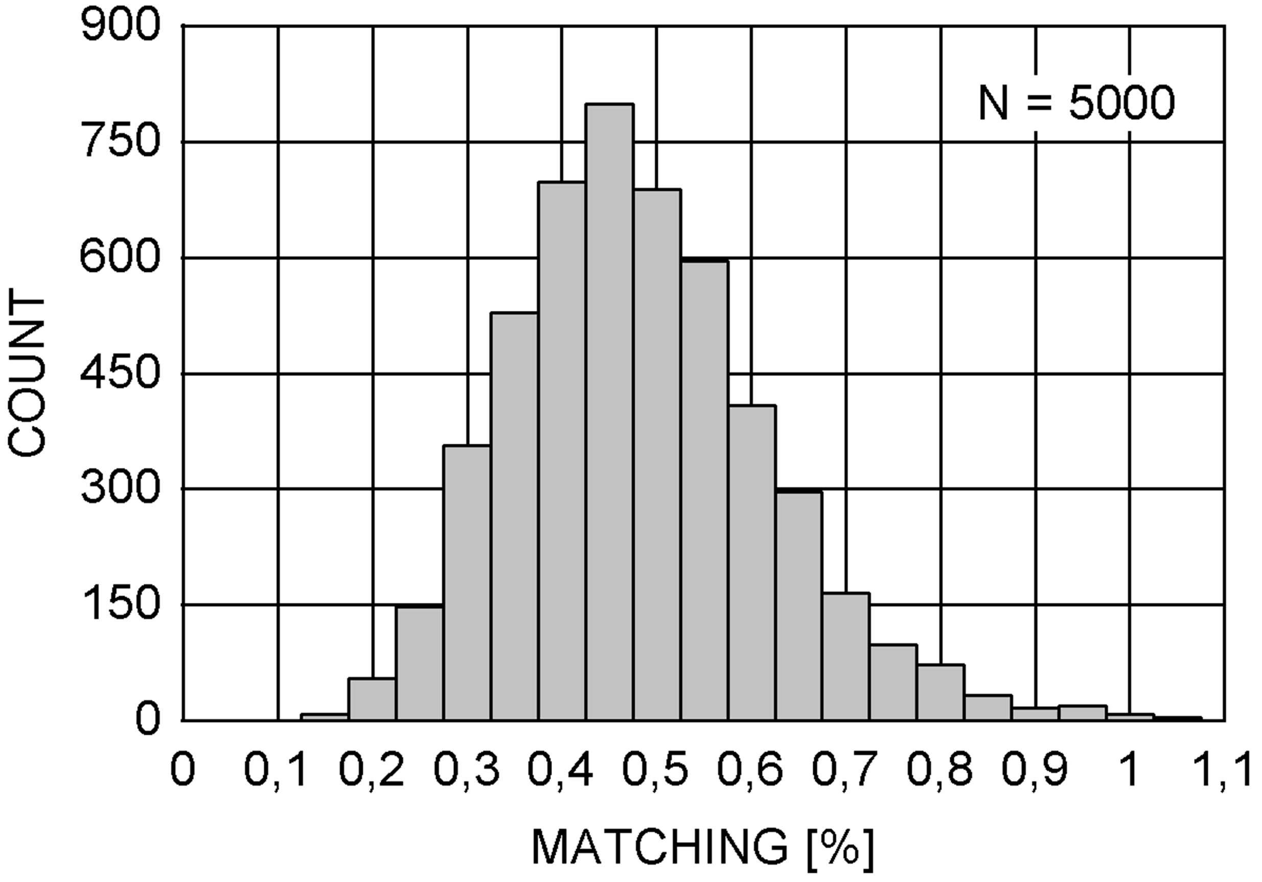
| IMATCH | Matching (2) | Output current set to 17.5 mA TA = 25°C |
1% | 2.5% | ||
| ƒLED | LED switching frequency | 312 | Hz | |||
| VSAT | Saturation voltage (3) | Output current set to 17.5 mA TA = 25°C |
45 | 100 | mV | |
(1) Low-ESR Surface-Mount Ceramic Capacitors (MLCCs) used in setting electrical characteristics.
(2) Output Current Accuracy is the difference between the actual value of the output current and programmed value of this current. Matching is the maximum difference from the average. For the constant current outputs on the part (D1 to D9), the following are determined: the maximum output current (MAX), the minimum output current (MIN), and the average output current of all outputs (AVG). Two matching numbers are calculated: (MAX-AVG)/AVG and (AVG-MIN)/AVG. The largest number of the two (worst case) is considered the matching figure. Note that some manufacturers have different definitions in use.
(3) Saturation voltage is defined as the voltage when the LED current has dropped 10% from the value measured at VOUT – 1V.
6.8 LED Test Electrical Characteristics
Typical (TYP) values apply for TA = 25°C and minimum (MIN) and maximum (MAX) apply over the operating ambient temperature range (−30°C < TA < 85°C). Specifications apply to the LP55231 Functional Block Diagram with: VDD = 3.6 V, VEN = 1.65 V, COUT = 1 µF, CIN = 1 µF, C1–2 = 0.47 µF, unless otherwise specified.(1)| PARAMETER | TEST CONDITIONS | MIN | TYP | MAX | UNIT | |
|---|---|---|---|---|---|---|
| LSB | Least significant bit | 30 | mV | |||
| EABS | Total unadjusted error(2) | VIN_TEST = 0V to VDD
TA = 25°C |
< ±3 | ±4 | LSB | |
| tCONV | Conversion time | 2.7 | ms | |||
| VIN_TEST | DC voltage range | TA = 25°C | 0 | 5 | V | |
(1) Low-ESR Surface-Mount Ceramic Capacitors (MLCCs) used in setting electrical characteristics.
(2) Total unadjusted error includes offset, full-scale, and linearity errors.
6.9 Logic Interface Characteristics
Typical (TYP) values apply for TA = 25°C and minimum (MIN) and maximum (MAX) apply over the operating ambient temperature range (−30°C < TA < 85°C). Specifications apply to the LP55231 Functional Block Diagram with: VDD = 3.6 V, VEN = 1.65 V, COUT = 1 µF, CIN = 1 µF, C1–2 = 0.47 µF, unless otherwise specified.(1)| PARAMETER | TEST CONDITIONS | MIN | TYP | MAX | UNIT | |
|---|---|---|---|---|---|---|
| LOGIC INPUT EN | ||||||
| VIL | Input low level | 0.5 | V | |||
| VIH | Input high level | 1.2 | V | |||
| II | Input current | –1 | 1 | µA | ||
| tDELAY | Input delay(2) | 2 | µs | |||
| LOGIC INPUT SCL, SDA, TRIG, CLK, ASEL0, ASEL1 | ||||||
| VIL | Input low level | 0.2xVEN | V | |||
| VIH | Input high level | 0.8xVEN | V | |||
| II | Input current | –1 | 1 | µA | ||
| LOGIC OUTPUT SDA, TRIG, INT | ||||||
| VOL | Output low level | IOUT = 3 mA (pullup current) | 0.3 | 0.5 | V | |
| IL | Output leakage current | VOUT = 2.8 V | 1 | µA | ||
(1) Low-ESR Surface-Mount Ceramic Capacitors (MLCCs) used in setting electrical characteristics.
(2) The I2C host should allow at least 500 μs before sending data to the LP55231 after the rising edge of the enable line.
6.10 Recommended External Clock Source Conditions(1)(2)
| MIN | NOM | MAX | UNIT | |||
|---|---|---|---|---|---|---|
| LOGIC INPUT CLK | ||||||
| ƒCLK | Clock frequency | 32.7 | kHz | |||
| tCLKH | High time | 6 | µs | |||
| tCLKL | Low time | 6 | µs | |||
| tr | Clock rise time | 10% to 90% | 2 | µs | ||
| tf | Clock fall time | 90% to 10% | 2 | µs | ||
(1) Specification is verified by design and is not tested in production. VEN = 1.65 V to VDD.
(2) The ideal external clock signal for the LP55231 is a 0-V to VEN 25% to 75% duty-cycle square wave. At frequencies above 32.7 kHz, program execution will be faster, and at frequencies below 32.7 kHz program execution will be slower.
6.11 Serial Bus Timing Parameters (SDA, SCL)(1)
| MIN | MAX | UNIT | ||
|---|---|---|---|---|
| ƒSCL | Clock frequency | 400 | kHz | |
| 1 | Hold time (repeated) START condition | 0.6 | µs | |
| 2 | Clock low time | 1.3 | µs | |
| 3 | Clock high time | 600 | ns | |
| 4 | Setup time for a repeated START condition | 600 | ns | |
| 5 | Data hold time | 50 | ns | |
| 6 | Data setup time | 100 | ns | |
| 7 | Rise time of SDA and SCL | 20+0.1 Cb | 300 | ns |
| 8 | Fall time of SDA and SCL | 15+0.1 Cb | 300 | ns |
| 9 | Setup time for STOP condition | 600 | ns | |
| 10 | Bus free time between a STOP and a START condition | 1.3 | µs | |
| Cb | Capacitive load parameter for each bus line Load of One picofarad corresponds to one nanosecond. |
10 | 200 | ns |
(1) Specification is verified by design and is not tested in production. VEN = 1.65 V to VDD.
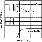
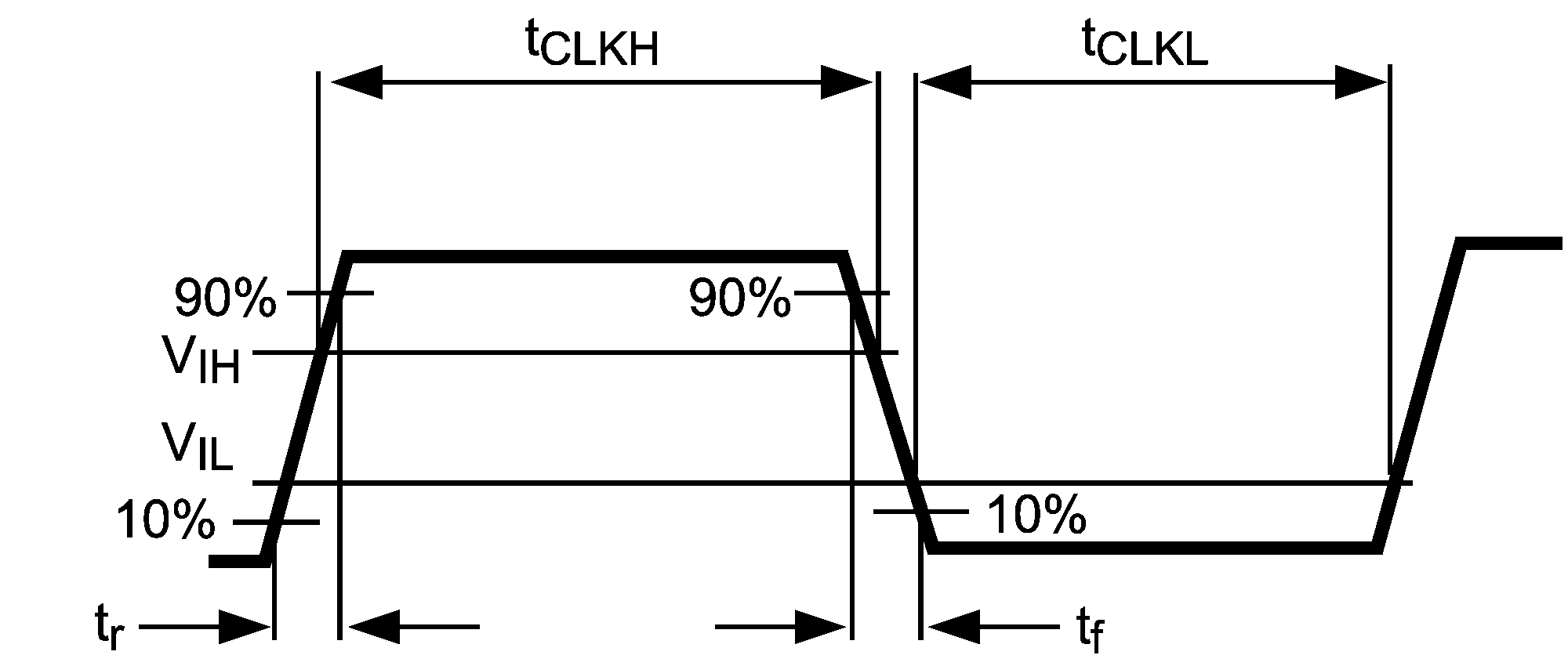 Figure 1. External Clock Signal
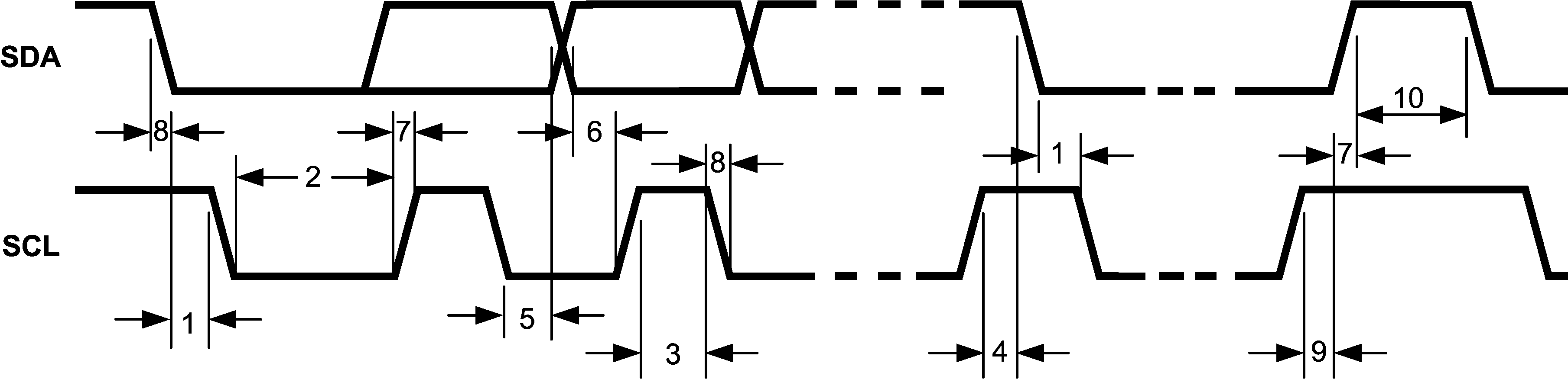 Figure 2. Timing Parameters
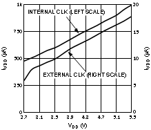
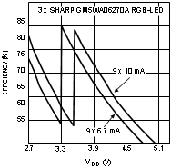
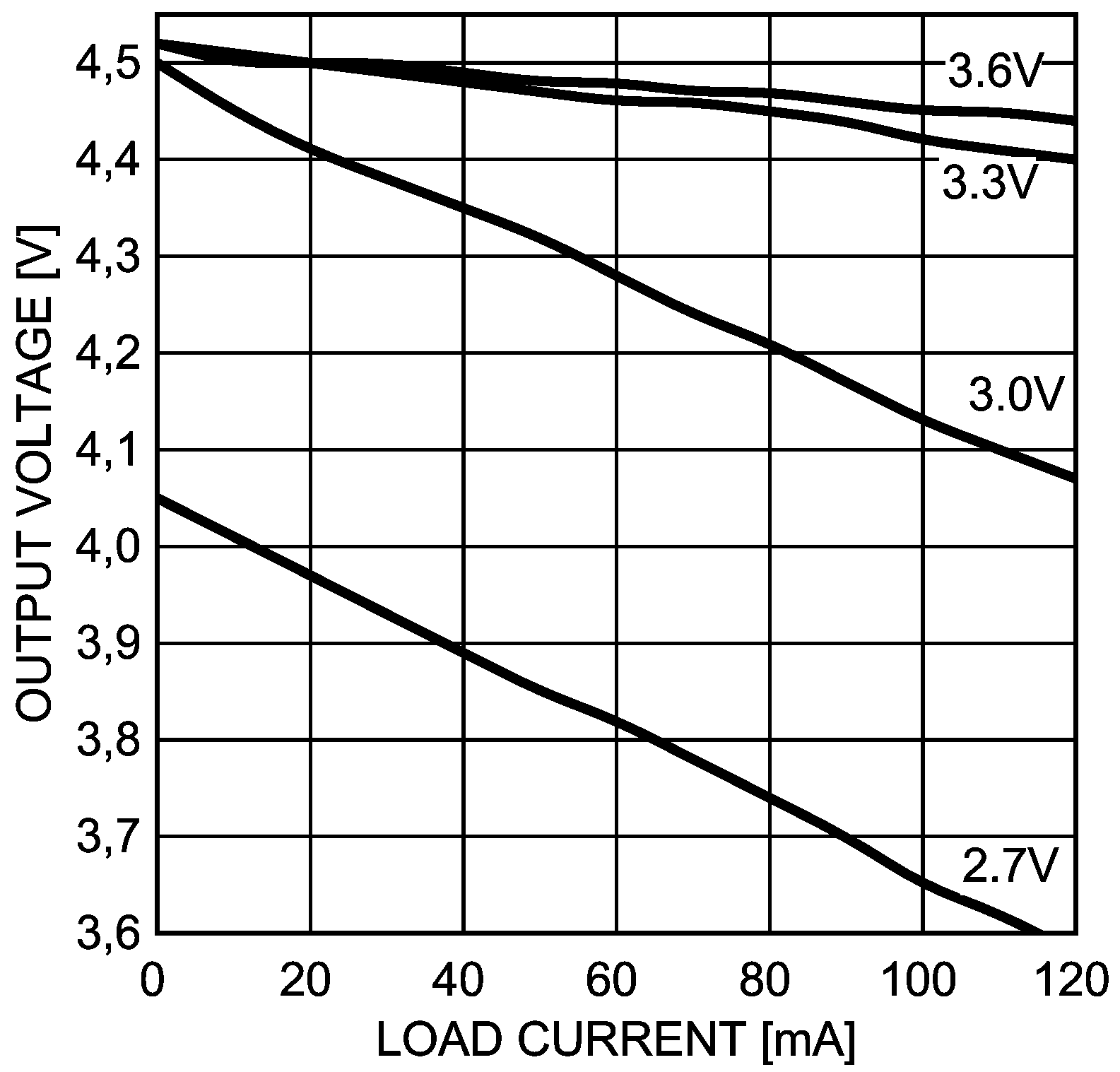
6.12 Typical Characteristics
Unless otherwise specified: VDD = 3.6 V, CIN = COUT = 1 µF, C1 = C2 = 0.47 µF, TA = 25°C. CIN, COUT, C1, C2: Low-ESR surface-mount ceramic capacitors (MLCCs) used in setting electrical characteristics.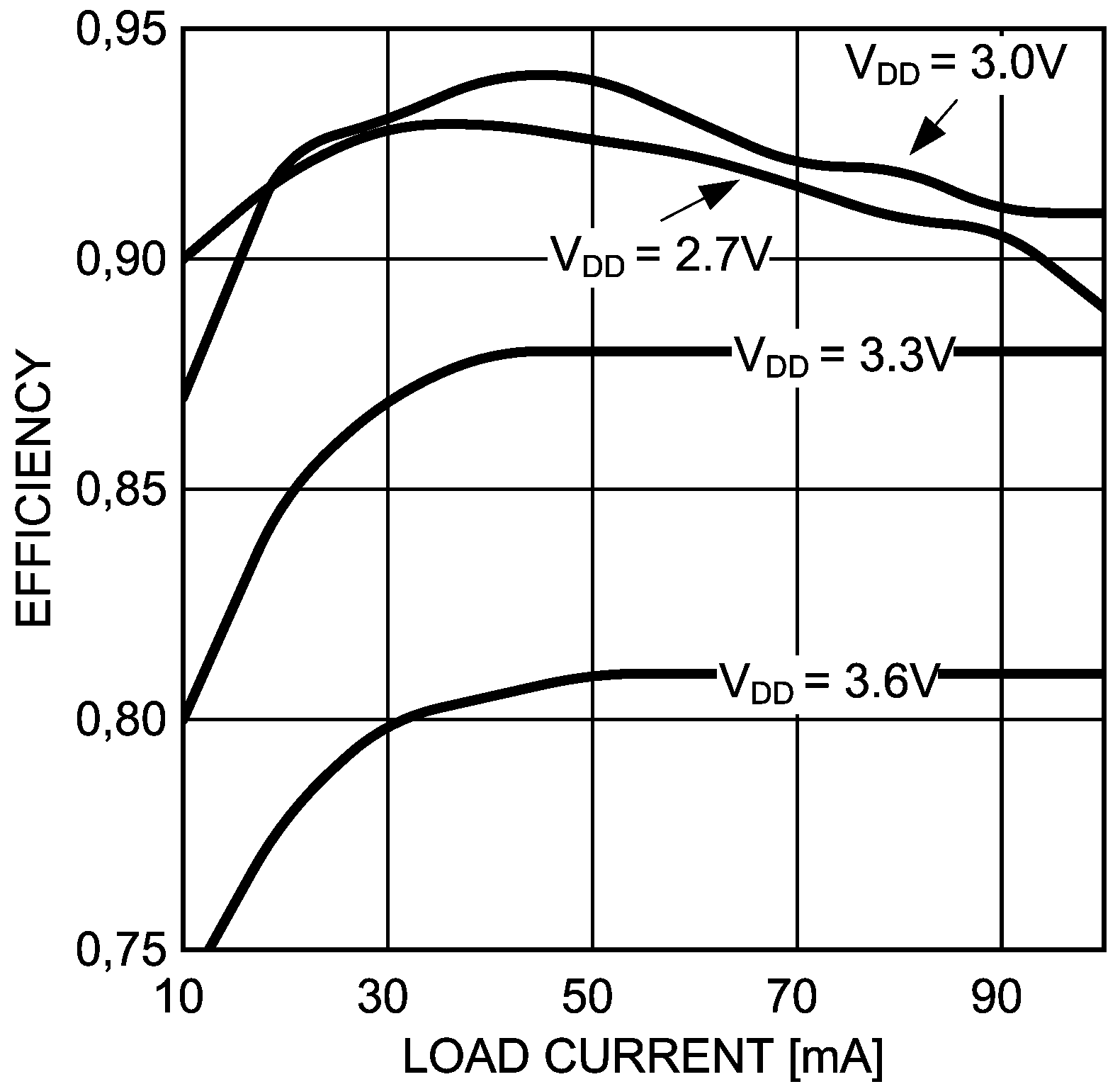
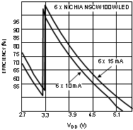
| 6 x 1-mA Load (6 Nichia NSCW100 WLEDs On D1 To D6) | ||
| 17.5 mA Current | ||
| Charge Pump In 1x Mode | ||
| If the charge pump is OFF the supply current is even lower. | ||
| Load: 6 x Nichia NSCW100 WLEDs On D1 To D6 @ 100% PWM | ||
| 17.5 mA Current | ||
| 51h To Addr 36h | ILOAD = 60 mA | VDD= 3.6 V |