ZHCSD18A March 2013 – October 2014 LP55231
PRODUCTION DATA.
- 1 特性
- 2 应用
- 3 说明
- 4 修订历史记录
- 5 Pin Configuration and Functions
-
6 Specifications
- 6.1 Absolute Maximum Ratings
- 6.2 Handling Ratings
- 6.3 Recommended Operating Conditions
- 6.4 Thermal Information
- 6.5 Electrical Characteristics
- 6.6 Charge Pump Electrical Characteristics
- 6.7 LED Driver Electrical Characteristics
- 6.8 LED Test Electrical Characteristics
- 6.9 Logic Interface Characteristics
- 6.10 Recommended External Clock Source Conditions
- 6.11 Serial Bus Timing Parameters (SDA, SCL)
- 6.12 Typical Characteristics
-
7 Detailed Description
- 7.1 Overview
- 7.2 Functional Block Diagram
- 7.3 Feature Description
- 7.4 Device Functional Modes
- 7.5 Programming
- 7.6 Register Maps
- 8 Application and Implementation
- 9 Power Supply Recommendations
- 10Layout
- 11器件和文档支持
- 12机械封装和可订购信息
5 Pin Configuration and Functions
WQFN (RTW)
24 Pins
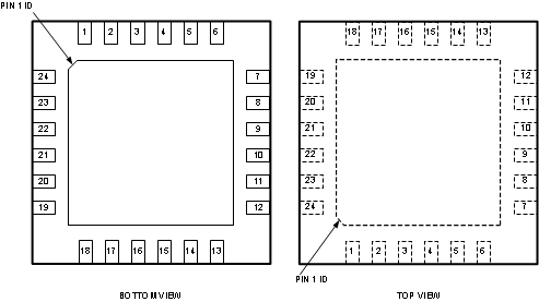
Pin Functions
| PIN | TYPE(1) | DESCRIPTION | |
|---|---|---|---|
| NUMBER | NAME | ||
| 1 | C2+ | A | Flying capacitor 2 positive terminal |
| 2 | C1+ | A | Flying capacitor 1 positive terminal |
| 3 | VDD | P | Input power supply |
| 4 | GND | G | Ground |
| 5 | EN | I | Enable |
| 6 | CLK | I | 32 kHz clock input. Connect to ground if not used |
| 7 | INT | OD/O | Interrupt for microcontroller unit. Leave unconnected if not used |
| 8 | SDA | I/OD | Serial interface data |
| 9 | SCL | I | Serial interface clock |
| 10 | TRIG | I/OD | Trigger. Connect to ground if not used |
| 11 | D9 | A | Current source output 9. Note: powered from VDD |
| 12 | D8 | A | Current source output 8. Note: powered from VDD |
| 13 | D7 | A | Current source output 7. Note: powered from VDD |
| 14 | D6 | A | Current source output 6 |
| 15 | D5 | A | Current source output 5 |
| 16 | D4 | A | Current source output 4 |
| 17 | D3 | A | Current source output 3 |
| 18 | D2 | A | Current source output 2 |
| 19 | D1 | A | Current source output 1 |
| 20 | ASEL0 | I | Serial interface address select input |
| 21 | ASEL1 | I | Serial interface address select input |
| 22 | VOUT | A | Charge pump output |
| 23 | C2− | A | Flying capacitor 2 negative terminal |
| 24 | C1− | A | Flying capacitor 1 negative terminal |
| DAP | Connect the die attach pad to GND | ||
(1) A: Analog Pin; G: Ground Pin; P: Power Pin; I: Input Pin; I/O Input/Output Pin; O: Output Pin; OD: Open Drain Pin