SNVS256D Novmeber 2003 – November 2016 LP3943
PRODUCTION DATA.
- 1 Features
- 2 Applications
- 3 Description
- 4 Revision History
- 5 Pin Configuration and Functions
- 6 Specifications
- 7 Detailed Description
- 8 Application and Implementation
- 9 Power Supply Recommendations
- 10Layout
- 11Device and Documentation Support
- 12Mechanical, Packaging, and Orderable Information
7 Detailed Description
7.1 Overview
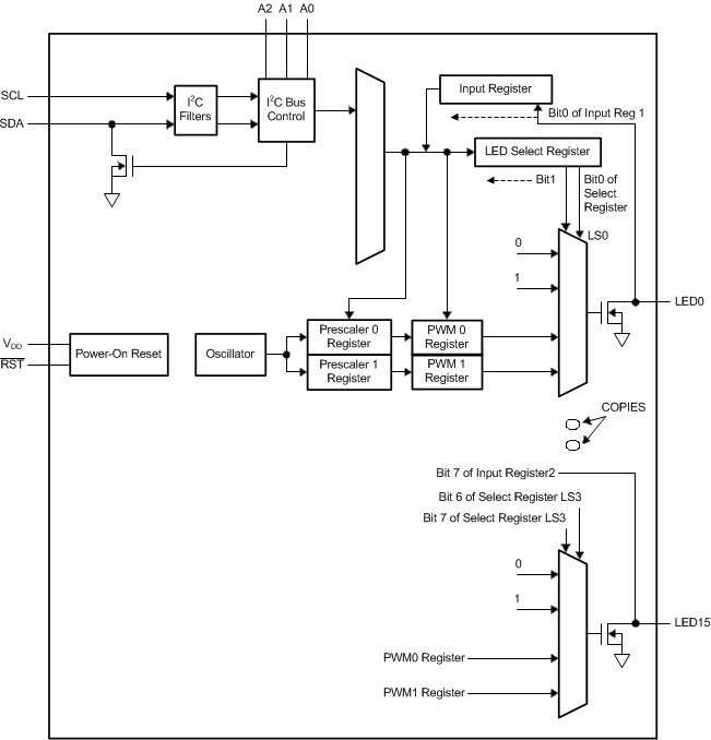
The LP3943 takes incoming data from the baseband controller and feeds them into several registers that control the frequency and the duty cycle of the LEDs. Two prescaler registers and two PWM registers provide two individual rates to dim or blink the LEDs (for more information on these registers, refer to Table 1). Each LED can be programmed in one of four states: ON, OFF, DIM0 rate, or DIM1 rate. Two read-only registers provide status on all 16 LEDs. The LP3943 can be used to drive RGB LEDs and/or single-color LEDs to create a colorful, entertaining, and informative setting. Alternatively, it can also drive RGB LED as a flashlight. This is particularly suitable for accessory functions in cellular phones and toys. Any LED pins not used to drive LED can be used for general purpose parallel input/output (GPIO) expansion.
The LP3943 is equipped with power-on reset that holds the chip in a reset state until VDD reaches VPOR during power up. Once VPOR is achieved, the LP3943 comes out of reset and initializes itself to the default state.
To bring the LP3943 into reset, hold the RST pin LOW for a period of TW. This puts the chip into its default state. The LP3943 can only be programmed after RST signal is HIGH again.
7.3 Feature Description
Some of the features of the LP3943 device are:
- 16 low-side switches to control the current in 16 strings of LEDs with a maximum of 25 mA per switch or a maximum of 200 mA total.
- Programmable internal PWM dimming:
- Duty cycle control (8 bits). Any of the 16 current switches can be mapped to either PWM0 register or PWM1 register. Each register offers 8-bit PWM duty cycle control.
- PWM Frequency control (8 bits). Any of the 16 current switches can be mapped to either PSC0 register or PSC1 register. Each register offers 8-bit PWM frequency control from 0.625 Hz to 160 Hz.
- RESET input.
- Auto increment for I2C writes to reduce number of I2C clock pulses .
- The LP3943 provides for an externally selectable I2C slave address via the ADR0, ADR1, and ADR2 inputs. See Figure 4.
7.4 Device Functional Modes
- Output set to high impedance. This is set by programming bits [B0 and B1] to 00 in the LS0, LS1, LS2, or LS3 registers (see Table 2)
- Output set to ON state (current switch pulls low). This turns the LED on at the full current in the specified current switch bits [B0 and B1] set to 01 in the LS0, LS1, LS2, or LS3 registers (see Table 12).
- Output set to toggle at the programmed PWM duty cycle and PWM frequency. This turns on or off the specified current switch at the programmed PWM frequency and duty cycle. Each current switch is mapped to either of the PWM0/PSC0 or PWM1/PSC1 pairs by setting [B0 and B1] to 10 or 11 in the LS0, LS1, LS2, or LS3 registers (see Table 12).
7.5 Programming
7.5.1 I2C Data Validity
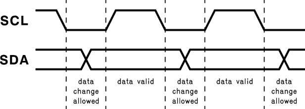
The data on SDA line must be stable during the HIGH period of the clock signal (SCL). In other words, state of the data line can only be changed when CLK is LOW.
 Figure 2. I2C Data Validity
7.5.2 I2C START and STOP Conditions
START and STOP bits classify the beginning and the end of the I2C session. START condition is defined as SDA signal transitioning from HIGH to LOW while SCL line is HIGH. STOP condition is defined as the SDA transitioning from LOW to HIGH while SCL is HIGH. The I2C master always generates START and STOP bits. The I2C bus is considered to be busy after START condition and free after STOP condition. During data transmission, I2C master can generate repeated START conditions. First START and repeated START conditions are equivalent, function-wise.
 Figure 3. I2C START and STOP Conditions
7.5.3 Transferring Data
Every byte put on the SDA line must be eight bits long with the most significant bit (MSB) being transferred first. The number of bytes that can be transmitted per transfer is unrestricted. Each byte of data has to be followed by an acknowledge bit. The acknowledge related clock pulse is generated by the master. The transmitter releases the SDA line (HIGH) during the acknowledge clock pulse. The receiver must pull down the SDA line during the 9th clock pulse, signifying an acknowledge. A receiver which has been addressed must generate an acknowledge after each byte has been received.
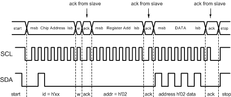
After the START condition, a chip address is sent by the I2C master. This address is seven bits long followed by an eighth bit which is a data direction bit (R/W). The LP3943 hardwires bits 7 to 4 and leaves bits 3 to 1 selectable, as shown in Figure 4. For the eighth bit, a “0” indicates a WRITE and a “1” indicates a READ. The LP3943 supports only a WRITE during chip addressing. The second byte selects the register to which the data is written. The third byte contains data to write to the selected register.
 Figure 4. Chip Address Byte

r = read (SDA = “1”)
ack = acknowledge (SDA pulled LOW by either master or slave)
rs = repeated start
xx = 60 to 67
However, if a READ function is to be accomplished, a WRITE function must precede the READ function, as shown in Figure 6.

r = read (SDA = “1”)
ack = acknowledge (SDA pulled LOW by either master or slave)
rs = repeated start
xx = 60 to 67
7.5.4 Auto Increment
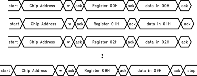
Auto increment is a special feature supported by the LP3943 to eliminate repeated chip and register addressing when data are to be written to or read from registers in sequential order. The auto increment bit is inside the register address byte, as shown in Figure 7. Auto increment is enabled when this bit is programmed to “1” and disabled when it is programmed to “0”.
Bits 5, 6 and 7 in the register address byte must always be zero.
 Figure 7. Register Address Byte
In the READ mode, when auto increment is enabled, I2C master could receive any number of bytes from LP3943 without selecting chip address and register address again. Every time the I2C master reads a register, the LP3943 increments the register address, and the next data register is read. When I2C master reaches the last register (09H), the register address rolls over to 00H.
In the WRITE mode, when auto increment is enabled, the LP3943 increments the register address every time I2C master writes to register. When the last register (09H register) is reached, the register address rolls over to 02H, not 00H, because the first two registers in LP3943 are read-only registers. It is possible to write to the first two registers independently, and the LP3943 device will acknowledge, but the data is ignored.
If auto increment is disabled, and the I2C master does not change register address, it continues to write data into the same register.
 Figure 8. Programming With Auto Increment Disabled (in WRITE Mode)
 Figure 9. Programming With Auto Increment Enabled (in WRITE Mode)
7.6 Register Maps
Table 1. LP3943 Register Table
| Address (Hex) | Register Name | Read/Write | Register Function |
|---|---|---|---|
| 0x00 | Input 1 | Read Only | LED0–7 Input Register |
| 0x01 | Input 2 | Read Only | LED8–15 Input Register |
| 0x02 | PSC0 | R/W | Frequency Prescaler 0 |
| 0x03 | PWM0 | R/W | PWM Register 0 |
| 0x04 | PSC1 | R/W | Frequency Prescaler 1 |
| 0x05 | PWM1 | R/W | PWM Register 1 |
| 0x06 | LS0 | R/W | LED0–3 Selector |
| 0x07 | LS1 | R/W | LED4–7 Selector |
| 0x08 | LS2 | R/W | LED8–11 Selector |
| 0x09 | LS3 | R/W | LED12–15 Selector |
7.6.1 Binary Format for Input Registers (Read-only)—Address 0x00 and 0x01
Table 2. Address 0x00
| Bit # | 7 | 6 | 5 | 4 | 3 | 2 | 1 | 0 |
| Default value | X | X | X | X | X | X | X | X |
| LED7 | LED6 | LED5 | LED4 | LED3 | LED2 | LED1 | LED0 |
Table 3. Address 0x01
| Bit # | 7 | 6 | 5 | 4 | 3 | 2 | 1 | 0 |
| Default value | X | X | X | X | X | X | X | X |
| LED15 | LED14 | LED13 | LED12 | LED11 | LED10 | LED9 | LED8 |
7.6.2 Binary Format for Frequency Prescaler and PWM Registers — Address 0x02 to 0x05
Table 4. Address 0x02 (PSC0)
| Bit # | 7 | 6 | 5 | 4 | 3 | 2 | 1 | 0 |
| Default value | 0 | 0 | 0 | 0 | 0 | 0 | 0 | 0 |
Table 5. Address 0x03 (PWM0)
| Bit # | 7 | 6 | 5 | 4 | 3 | 2 | 1 | 0 |
| Default value | 1 | 0 | 0 | 0 | 0 | 0 | 0 | 0 |
Table 6. Address 0x04 (PSC1)
| Bit # | 7 | 6 | 5 | 4 | 3 | 2 | 1 | 0 |
| Default value | 0 | 0 | 0 | 0 | 0 | 0 | 0 | 0 |
Table 7. Address 0x05 (PWM1)
| Bit # | 7 | 6 | 5 | 4 | 3 | 2 | 1 | 0 |
| Default value | 1 | 0 | 0 | 0 | 0 | 0 | 0 | 0 |
7.6.3 Binary Format for Selector Registers — Address 0x06 to 0x09
Table 8. Address 0x06 (LS0)
| Bit # | 7 | 6 | 5 | 4 | 3 | 2 | 1 | 0 |
| Default value | 0 | 0 | 0 | 0 | 0 | 0 | 0 | 0 |
| B1 | B0 | B1 | B0 | B1 | B0 | B1 | B0 | |
| LED3 | LED2 | LED1 | LED0 | |||||
Table 9. Address 0x07 (LS1)
| Bit # | 7 | 6 | 5 | 4 | 3 | 2 | 1 | 0 |
| Default value | 0 | 0 | 0 | 0 | 0 | 0 | 0 | 0 |
| B1 | B0 | B1 | B0 | B1 | B0 | B1 | B0 | |
| LED7 | LED6 | LED5 | LED4 | |||||
Table 10. Address 0x08 (LS2)
| Bit # | 7 | 6 | 5 | 4 | 3 | 2 | 1 | 0 |
| Default value | 0 | 0 | 0 | 0 | 0 | 0 | 0 | 0 |
| B1 | B0 | B1 | B0 | B1 | B0 | B1 | B0 | |
| LED11 | LED10 | LED9 | LED8 | |||||
Table 11. Address 0x09 (LS3)
| Bit # | 7 | 6 | 5 | 4 | 3 | 2 | 1 | 0 |
| Default value | 0 | 0 | 0 | 0 | 0 | 0 | 0 | 0 |
| B1 | B0 | B1 | B0 | B1 | B0 | B1 | B0 | |
| LED15 | LED14 | LED13 | LED12 | |||||
Table 12. LED States With Respect To Values in B1 and B0
| B1 | B0 | Function |
|---|---|---|
| 0 | 0 | Output Hi-Z (LED off) |
| 0 | 1 | Output LOW (LED on) |
| 1 | 0 | Output dims (DIM0 rate) |
| 1 | 1 | Output dims (DIM1 rate) |
Programming Example:
- Dim LEDs 0 to 7 at 1 Hz at 25% duty cycle
- Dim LEDs 8 to 12 at 5 Hz at 50% duty cycle
- Set LEDs 13, 14 and 15 off
- Step 1: Set PSC0 to achieve DIM0 of 1 s
- Step 2: Set PWM0 duty cycle to 25%
- Step 3: Set PSC1 to achieve DIM1 of 0.2 s
- Step 4: Set PWM1 duty cycle to 50%
- Step 5: Set LEDs 13, 14 and 15 off by loading the data into LS3 register
- Step 6: Set LEDs 0 to 7 to point to DIM0
- Step 7: Set LEDs 8 to 12 to point to DIM1
Table 13. Programming Details
| STEP | DESCRIPTION | REGISTER NAME | SET TO (HEX) |
|---|---|---|---|
| 1 | Set DIM0 = 1 s 1 = (PSC0 + 1)/160 PSC0 = 159 |
PSC0 | 0x09F |
| 2 | Set duty cycle to 25% Duty Cycle = PWM0/256 PWM0 = 64 |
PWM0 | 0x40 |
| 3 | Set DIM1 = 0.2s 0.2 = (PSC1 + 1)/160 PSC1 = 31 |
PSC1 | 0x1F |
| 4 | Set duty cycle to 50% Duty Cycle = PWM1/256 PWM1 = 128 |
PWM1 | 0x80 |
| 5 | LEDs 13, 14 and 15 off Output = HIGH |
LS3 | 0x03 |
| 6 | LEDs 0 to 7 Output = DIM0 |
LS0, LS1 | LS0 = 0xAA LS1 = 0xAA |
| 7 | LEDs 8 to 12 Output = DIM1 |
LS2, LS3 | LS2 = 0xFF LS3 = 0x03 |
