SNVS256D Novmeber 2003 – November 2016 LP3943
PRODUCTION DATA.
- 1 Features
- 2 Applications
- 3 Description
- 4 Revision History
- 5 Pin Configuration and Functions
- 6 Specifications
- 7 Detailed Description
- 8 Application and Implementation
- 9 Power Supply Recommendations
- 10Layout
- 11Device and Documentation Support
- 12Mechanical, Packaging, and Orderable Information
8 Application and Implementation
NOTE
Information in the following applications sections is not part of the TI component specification, and TI does not warrant its accuracy or completeness. TI’s customers are responsible for determining suitability of components for their purposes. Customers should validate and test their design implementation to confirm system functionality.
8.1 Application Information
The LP3943 is a 16-channel LED controller which has 16 low-side current switches. Each switch can control the LED current in its respective LED or LEDs by modulating its duty cycle and frequency.
8.2 Typical Application
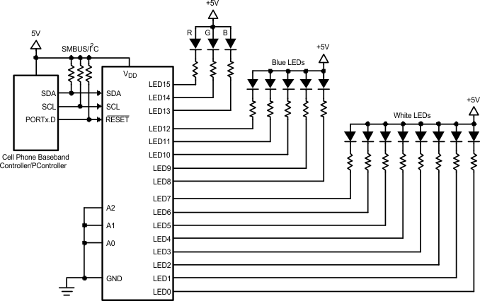
 Figure 10. LP3943 Typical Application
8.2.1 Design Requirements
For typical RGB LED light-driver applications, use the parameters listed in Table 14.
Table 14. Design Parameters
| DESIGN PARAMETER | EXAMPLE VALUE |
|---|---|
| Minimum input voltage | 2.3 V |
| Typical output voltage | 5 V |
| Output current | 20 mA |
8.2.2 Detailed Design Procedure
8.2.2.1 Reducing IQ When LEDs are OFF
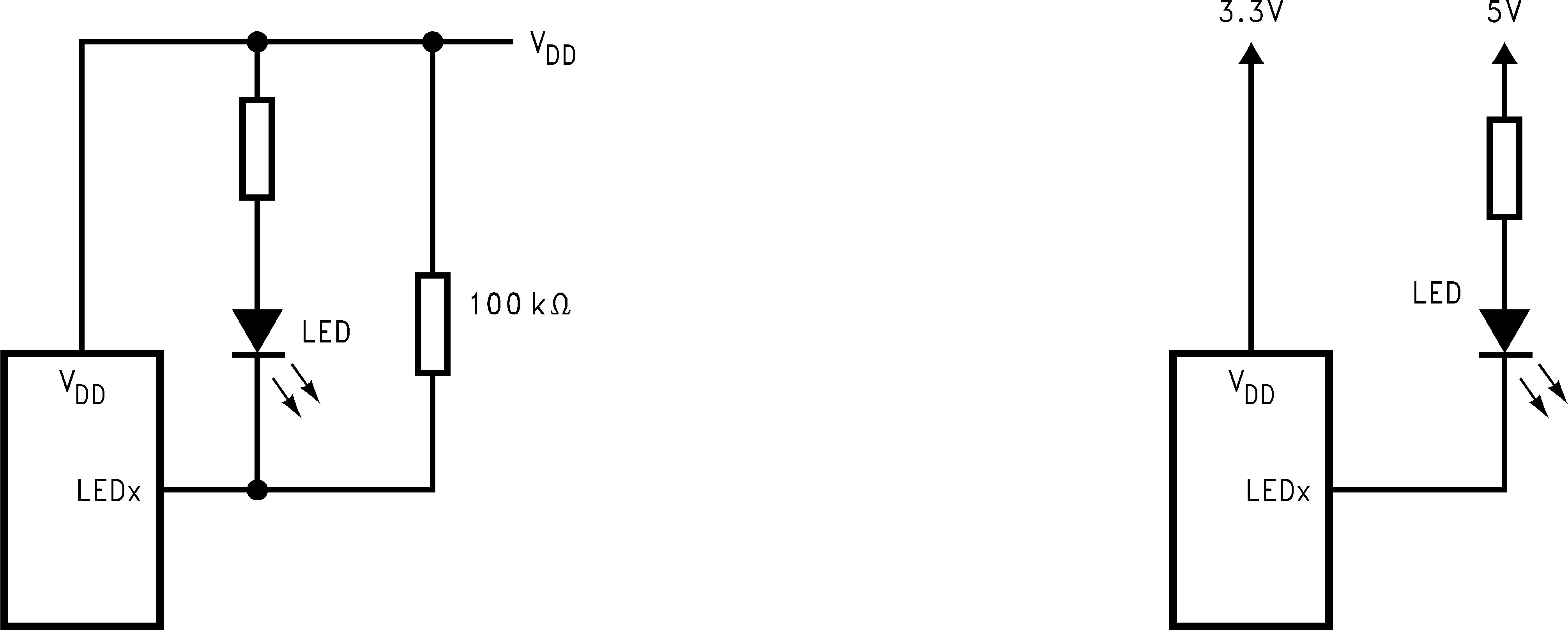
In many applications, the LEDs and the LP3943 share the same VDD, as shown in Figure 10. When the LEDs are off, the LED pins are at a lower potential than VDD, causing extra supply current (ΔIQ). To minimize this current, consider keeping the LED pins at a voltage equal to or greater than VDD.
 Figure 11. Methods to Reduce IQ When LEDs are in OFF State
8.2.3 Application Curve
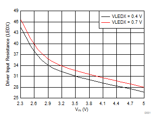
 Figure 12. Typical LED Switch Resistance
8.3 System Examples
 Figure 13. LP3943 With 5-V Booster
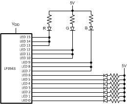
 Figure 14. LP3943 Driving RGB LED as a Flash