SNVS337F June 2006 – September 2015 LP38859
PRODUCTION DATA.
- 1 Features
- 2 Applications
- 3 Description
- 4 Revision History
- 5 Specifications
- 6 Detailed Description
- 7 Application and Implementation
- 8 Power Supply Recommendations
- 9 Layout
- 10Device and Documentation Support
- 11Mechanical, Packaging, and Orderable Information
封装选项
机械数据 (封装 | 引脚)
散热焊盘机械数据 (封装 | 引脚)
- KTT|5
订购信息
6 Detailed Description
6.1 Overview
The LP38559 is a fast-response, high-current, low-dropout regulator, available in output voltages are 0.8 V and 1.2 V. This part is capable of delivering 3-A continuous load current. Standard regulator features, such as overcurrent and over temperature protection, are also included. The LP38559 contains several features:
- Low dropout voltage, typical 240 mV at 3-A load.
- The bias voltage(VBIAS) provides voltage to drive the gate of the N-MOS power transistor.
- The input voltage(VIN) is the input voltage which supplies power to the load.
- Programmable soft-start time.
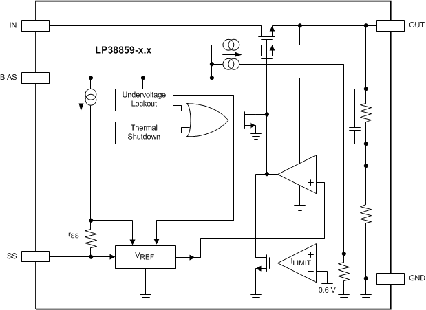
6.2 Functional Block Diagram

6.3 Feature Description
6.3.1 Input Voltage
The input voltage (VIN) is the high current external voltage rail that is regulated down to a lower voltage, which is applied to the load. The input voltage must be at least VOUT + VDO, and no higher than whatever values is used for VBIAS.
6.3.2 Bias Voltage
The bias voltage (VBIAS) is a low current external voltage rail required to bias the control circuitry and provide gate drive for the N-FET pass transistor. The bias voltage must be in the range of 3 V to 5.5 V to ensure proper operation of the device.
6.3.3 Undervoltage Lockout
The bias voltage is monitored by a circuit which prevents the device from functioning when the bias voltage is below the undervoltage lockout (UVLO) threshold of approximately 2.45 V.
As the bias voltage rises above the UVLO threshold the device control circuitry becomes active. There is approximately 150 mV of hysteresis built into the UVLO threshold to provide noise immunity.
When the bias voltage is between the UVLO threshold and the minimum operating rating value of 3 V, the device is functional, but the operating parameters are not within the specified limits.
6.3.4 Supply Sequencing
There is no requirement for the order that VIN or VBIAS are applied or removed.
One practical limitation is that the soft-start circuit starts charging CSS when VBIAS rises above the UVLO threshold. If the application of VIN is delayed beyond this point the benefits of soft start are compromised.
In any case, the output voltage cannot be specified until both VIN and VBIAS are within the range of specified operating values.
If used in a dual-supply system where the regulator output load is returned to a negative supply, the output pin must be diode clamped to ground. A Schottky diode is recommended for this diode clamp.
6.3.5 Reverse Voltage
A reverse voltage condition exists when the voltage at the output pin is higher than the voltage at the input pin. Typically this happens when VIN is abruptly taken low and COUT continues to hold a sufficient charge such that the input to output voltage becomes reversed.
The NMOS pass element, by design, contains no body diode. This means that, as long as the gate of the pass element is not driven, there is no reverse current flow through the pass element during a reverse voltage event. The gate of the pass element is not driven when VBIAS is below the UVLO threshold.
When VBIAS is above the UVLO threshold, the control circuitry is active and attempts to regulate the output voltage. Because the input voltage is less than the output voltage the control circuit drives the gate of the pass element to the full VBIAS potential when the output voltage begins to fall. In this condition, reverse current flows from the OUT pin to the IN pin , limited only by the RDS(ON) of the pass element and the output to input voltage differential. This condition is outside the specified operating range and must be avoided.
6.3.6 Soft-Start
The LP38859 incorporates a soft-start function that reduces the start-up current surge into the output capacitor (COUT) by allowing VOUT to rise slowly to the final value. This is accomplished by controlling VREF at the SS pin. The soft-start timing capacitor (CSS) is internally held to ground until VBIAS rises above the UVLO threshold.
VREF rises at an RC rate defined by the internal resistance of the SS pin (rSS), and the external capacitor connected to the SS pin. This allows the output voltage to rise in a controlled manner until steady-state regulation is achieved. Typically, five time constants are recommended to assure that the output voltage is sufficiently close to the final steady-state value. During the soft-start time the output current can rise to the built-in current limit.
Because the VOUT rise is exponential, not linear, the in-rush current peaks during the first time constant (τ), and VOUT requires four additional time constants (4τ) to reach the final value (5τ) .
After achieving normal operation, if VBIAS falsl below the ULVO threshold, the device output is disabled, and the soft-start capacitor (CSS) discharge circuit becomes active. The CSS discharge circuit remains active until VBIAS falls to 500 mV (typical). When VBIAS falls below 500 mV (typical), the CSS discharge circuit ceases to function due to a lack of sufficient biasing to the control circuitry.
Because VREF appears on the SS pin, any leakage through CSS causes VREF to fall, and thus affect VOUT. A leakage of 50 nA (about 10 MΩ) through CSS causes VOUT to be approximately 0.1% lower than nominal, while a leakage of 500 nA (about 1 MΩ) causes VOUT to be approximately 1% lower than nominal. Typical ceramic capacitors have a factor of 10× difference in leakage between 25°C and 85°C, so the maximum ambient temperature must be included in the capacitor selection process.
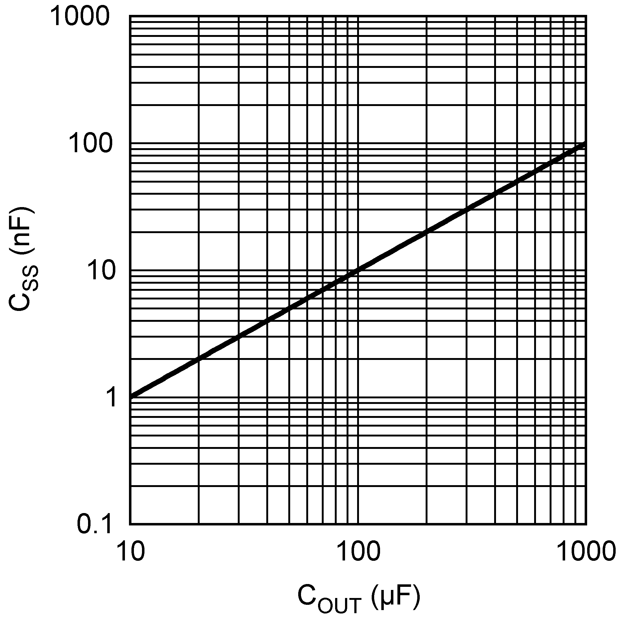
Typical CSS values are in the range of 1 nF to 100 nF, providing typical soft-start times in the range of 70 μs to 7 ms (5τ). Values less than 1 nF can be used, but the soft-start effect is minimal. Values larger than 100 nF provide soft start, but may not be fully discharged if VBIAS falls from the UVLO threshold to less than 500 mV in less than 100 µs.
Figure 19 shows the relationship between the COUT value and a typical CSS value.
 Figure 19. Typical CSS vs COUT Values
The CSS capacitor must be connected to a clean ground path back to the device ground pin. No components, other than CSS, should be connected to the SS pin, as there could be adverse effects to VOUT.
If the soft-start function is not needed, the SS pin must be left open, although some minimal capacitance value is always recommended.
6.4 Device Functional Modes
6.4.1 Operation with 3 V ≤ VBIAS ≤ 5.5 V, VOUT(TARGET)+ 0.3 V ≤ VIN ≤ VBIAS
The device operates if the bias voltage is equal to, or exceeds, 3 V, and input voltage is equal to, or exceeds, VOUT(TARGET) + 0.3 V. At bias voltages below the minimum VBIAS requirement, the device does not operate correctly, and output voltage may not reach target value.